



Part 10 — Assignment-1 Fully Solved
Last-Night Revision Sheet (COA)
Read This First
What this subject is about, in plain words
You use a computer every day, but what actually happens inside when you press “=” on the calculator app? Computer Organization and Architecture (COA) explains the inside of a computer: how numbers are stored as 0s and 1s, how the processor (CPU) fetches and runs instructions, how memory and input/output devices talk to it, and how engineers make all of this faster.
Analogy for the whole subject — a restaurant kitchen. - Memory = the store room (holds ingredients = data, and recipes = programs). - CPU = the head chef. Registers = the chef’s small worktable (tiny but instantly reachable). ALU = the chef’s hands that chop and mix (does arithmetic and logic). Control unit = the chef’s brain reading the recipe step by step. - Bus = the corridor through which ingredients are carried. - I/O devices = waiters bringing orders in and taking dishes out. - Pipelining = an assembly line where several dishes are at different stages at the same time. - Cache = a small fridge next to the chef holding the most-used ingredients.
Where the content comes from
Your folder had: nine unit PPTs (Units 1–9, the standard Morris Mano / GTU 3140707 syllabus), three sets of handwritten class notes (“COA Unit-1/2/3 Notes”), and Assignment-1. No official syllabus PDF for this subject was in the folder, so this guide covers everything in all of these:
| Part | Topics | Source |
|---|---|---|
| 0 | Architecture vs organization, functional units, buses, bus arbitration, timing, registers | Handwritten Unit 1 |
| 1 | Data representation, complements, fixed/floating point, register transfer, micro-operations | PPT Unit 1 + Handwritten Unit 2 |
| 2 | Adders, carry look-ahead, multiplication, division, floating- point arithmetic | Handwritten Unit 2 + PPT Unit 7 |
| 3 | Basic computer organization and design (Mano’s basic computer) | PPT Unit 2 + Handwritten Unit 3 |
| 4 | Programming the basic computer (assembly language) | PPT Unit 3 |
| 5 | Microprogrammed control (incl. horizontal/vertical) | PPT Unit 4 + Handwritten Unit 3 |
| 6 | Central Processing Unit (registers, stack, instruction formats, addressing modes, RISC/CISC) | PPT Unit 5 + Handwritten Unit 3 |
| 7 | Pipeline and vector processing (incl. reservation tables, collision vectors) | PPT Unit 6 + Handwritten Unit 3 |
| 8 | Input-output organization | PPT Unit 8 |
| 9 | Memory organization | PPT Unit 9 |
| 10 | All Assignment-1 questions solved | Assignment-1 |
Binary basics you need before starting (5-minute refresher)
Binary = base 2, digits 0 and 1 (bits). Each position is a power of 2:
| = base 2, digits | 0 and 1 (bits). | Each | position is | a power of | 2: | |||
|---|---|---|---|---|---|---|---|---|
| Position | 7 | 6 | 5 | 4 | 3 | 2 | 1 | 0 |
| Value | 128 | 64 | 32 | 16 | 8 | 4 | 2 | 1 |
1011₂ = 8 + 0 + 2 + 1 = 11. Decimal 37 → 32 + 4 + 1 → 00100101.
4 bits = a nibble, 8 bits = a byte, a word = the natural size the CPU handles (16, 32, 64 bits). Hexadecimal (base 16) = shorthand for binary, one hex digit = 4 bits: 1010 1111₂ = AF₁₆. With n bits you can make 2ⁿ different patterns. 10 bits → 1024 patterns. This fact is used in almost every numerical in this subject (“how many bits are needed to address 4096 words?”
→ 2¹² = 4096 → 12 bits).
Power
Value
Name
| 2¹⁰ | 1024 | 1 K |
|---|---|---|
| 2²⁰ | 1,048,576 | 1 M |
| 2³⁰ | ≈ 10⁹ | 1 G |
So 64K = 2⁶ × 2¹⁰ = 2¹⁶; 256K = 2¹⁸.
Binary addition rules: 0+0 = 0; 0+1 = 1; 1+1 = 10 (write 0, carry 1); 1+1+1 = 11 (write 1, carry 1).
Fundamentals: Architecture, Functional Units, Buses, Registers
0.1 Computer architecture vs computer organization (Assignment Q1)
Computer architecture = the attributes of a computer visible to the programmer — what the computer does. Examples: the instruction set, number of bits used to represent data, addressing modes, I/O mechanisms.
Computer organization = the operational units and their interconnections that realise the architecture — how it does it. Examples: control signals, interfaces, memory technology, whether multiplication is done by a dedicated multiplier circuit or by repeated addition.
Analogy: Architecture is the building plan a client sees (number of rooms, where the doors are). Organization is the construction details (type of bricks, wiring routes). Two buildings with the same plan can be built differently. Real example: Intel Core i3 and Core i9 have the same architecture (x86-64 — the same programs run on both) but different organization (cache sizes, number of cores, pipeline design).
| Basis | Architecture | Organization |
|---|---|---|
| Question answered | What does the computer do? | How does it do it? |
| Visible to programmer? | Yes | No (transparent) |
| Deals with | Instruction set, data types, addressing modes | Control signals, circuits, memory technology |
| Level | High-level design | Low-level implementation |
| Decided | First | After the architecture |
0.2 Functional units of a computer
Every digital computer has five functional units:
 ┌──────────────┐ ┌─────────────┐ ┌──────────┐
 │ Processor │ │ Memory │ │ Input │
 │ ALU │ │ │ │ unit │
 │ CU │ │ │ │ │
 │ Registers │ │ │ │ │
 └──────┬───────┘ └──────┬──────┘ └────┬─────┘
 │ │ │
 ═════════════╧═════════ BUS INTERCONNECTION ══════════╧════════
 │
 ┌──────┴──────┐
 │ Output unit │
 └─────────────┘
-
Input unit — accepts data/programs from outside (keyboard, mouse, scanner, sensors) and converts them to binary.
-
Memory unit — stores programs and data. Primary (main) memory = RAM, fast, directly accessed by the CPU, volatile. Secondary memory = disks, slower, permanent, large.
-
ALU (Arithmetic Logic Unit) — performs arithmetic (add, subtract, multiply, divide) and logic (AND, OR, NOT, compare) operations.
-
Control unit (CU) — the “manager”: fetches instructions, decodes them, and sends control signals (timing and command signals) telling every other unit what to do and when.
-
Output unit — sends results outside (monitor, printer, speakers).
CPU = ALU + CU + registers. All units are connected by the bus.
0.3 Buses
What is a bus?
A bus is a shared communication pathway connecting two or more devices. Physically it is a group of wires (lines); each line carries one bit (0 or 1) at a time. A bus connecting the major components (processor, memory, I/O) is called a system bus.
Key property: a bus is shared — if two devices put signals on it at the same moment, the signals collide and become garbage. So only one device transmits at a time (this is why we need bus arbitration, below).
The three groups of lines
| The three groups of | lines | ||
|---|---|---|---|
| Bus | Carries | Direction | Width determines |
| Data bus | the actual data being moved | Bidirectional (CPU ↔︎ memory/I/O) | how many bits are moved at once (affects performance) |
| Address bus | the address of the memory location or I/O port | Unidirectional (CPU → memory/I/O) | the maximum memory capacity: n address lines → 2ⁿ locations |
| Control bus | command and timing signals | Bidirectional (individual lines are one-way) | — |
Example: to read memory word 2000, the CPU puts 2000 on the address bus, activates Memory Read on the control bus, and the memory places the word on the data bus.
Address bus numerical: a CPU with a 16-bit address bus can address 2¹⁶ = 65,536 = 64 K locations. A 32-bit address bus → 2³² = 4 G locations.
Typical control lines: Memory Write, Memory Read, I/O Write, I/O Read, Transfer ACK, Bus Request, Bus Grant, Interrupt Request, Interrupt ACK, Clock, Reset.
Timing signals indicate when data and addresses are valid.
Command signals specify which operation to perform.
Types of buses
Dedicated bus: permanently assigned to one function or to one subset of components (separate address and data lines). Faster, more wires.
Multiplexed bus: the same lines are used for different purposes at different times — e.g., at the start of a transfer the lines carry the address, then the same lines carry the data (an Address Valid control line tells which). Fewer wires (cheaper) but slower and more complex control.
Bus structures
Single-bus structure: all units share one bus — simple and cheap, but only one transfer at a time → slow.
Multiple-bus structure: separate buses (e.g., a fast processor–memory bus and a slower I/O bus connected via a bridge) → parallel transfers, better performance.
0.4 Bus arbitration
The problem: several devices (CPU, DMA controller, I/O processor) may want to use the bus at the same time. The device that currently controls the bus is the bus master. Bus arbitration is
the process of deciding which device becomes the next bus master.
Two approaches:
Centralized arbitration — a single bus controller (arbiter) decides.
Distributed arbitration — all devices take part in the decision; no central arbiter.
(1) Daisy-chaining (centralized)
 Bus Busy ─────────────────────────────────────────
 Bus Request ──────┬────────────┬────────────┬─────
 ┌────────────┐ │ │ │
 │ Bus │ Bus Grant ┌────┴────┐ ┌────┴────┐ ┌────┴────┐
 │ controller │──────────▶│ Device 1 │─▶│ Device 2 │─▶│ Device 3 │
 └────────────┘ └─────────┘ └─────────┘ └─────────┘
 highest priority lowest priority
All devices share one Bus Request line. The Bus Grant signal passes from device to device in a chain.
When the controller sees a request, it sends Bus Grant to device 1. If device 1 requested, it keeps the grant and uses the bus; otherwise it passes it on to device 2, and so on. Priority is fixed by position — the device nearest the controller has the highest priority. ✔ Simple, few lines, easy to add devices. ✘ Low-priority devices may starve; if one device fails, devices after it are cut off; slow (signal passes through every device).
(2) Polling method (centralized)
The controller has poll-count lines (log₂ n lines for n devices). It puts device addresses on them one after another (a count).
When the polled device has a pending request, it activates Bus Busy and takes the bus. Priority can be changed just by changing the polling order (programmable).
✔ Flexible priority; a faulty device doesn’t block the others. ✘ More lines; polling takes time.
(3) Independent request (centralized)
Each device has its own Bus Request and Bus Grant line to the controller.
The controller sees all requests at once and grants the bus to the highest-priority one (via a built-in priority decoder).
✔ Fastest response; flexible priority. ✘ Most expensive — 2n lines for n devices.
(4) Distributed arbitration
Each device has a unique arbitration ID. Requesting devices put their IDs on shared arbitration lines; through a defined logic, the device with the highest ID wins.
✔ No single point of failure. ✘ More complex logic in every device.
| Method | Lines needed | Priority | Speed | Reliability |
|---|---|---|---|---|
| Daisy chain | 3 | Fixed by position | Slow | One failure breaks chain |
| Polling | log₂ n + 2 | Programmable | Medium | Good |
| Independent request | 2n | Programmable | Fastest | Good |
0.5 Bus timing
Timing = the way events on the bus are coordinated.
Synchronous timing:
All events are synchronised to a common clock signal on the bus.
Each transfer takes a fixed number of clock cycles; all devices read the clock line.
✔ Simple to design and test. ✘ Every device must run at the clock’s speed — the slowest device sets the pace.
 Clock _┌─┐_┌─┐_┌─┐_┌─┐_
 one cycle per event
Asynchronous timing:
No common clock. The occurrence of one event depends on the occurrence of the previous one, using handshaking signals (e.g., ready and acknowledge).
✔ Fast and slow devices can share the bus — each runs at its own speed. ✘ More complex control logic.
(Asynchronous data transfer with strobe and handshake is explained fully in Part 8.)
0.6 Registers
A register is a group of flip-flops inside the CPU; each flip-flop stores one bit. A 16-bit register stores 16 bits. Registers are the fastest storage in a computer (faster than cache and RAM) but very few in number.
Why are registers needed in a CPU? (Assignment Q2)
The ALU can only work on data that is close at hand; fetching every operand from memory would be very slow.
They hold instructions being executed, addresses being accessed, intermediate results of calculations, and the status of the processor.
They make the instruction cycle possible (PC, IR, MAR, MBR).
Types of registers
(a) User-visible registers (the programmer can use them in instructions):
General-purpose registers — hold data or addresses; any use (R0–R7).
Data registers — hold only data (e.g., the accumulator AC).
Address registers — hold addresses: segment pointers, index registers (for indexed addressing), stack pointer (top of the stack).
Condition codes (flags) — bits set by the hardware after operations (see PSW).
(b) Control and status registers (used by the control unit; mostly not directly visible):
PC (Program Counter) — holds the address of the next instruction to fetch.
IR (Instruction Register) — holds the instruction currently being executed.
MAR (Memory Address Register) — holds the address of the memory location to be read/written.
MDR / MBR (Memory Data / Buffer Register) — holds the data read from or to be written to memory.
PSW (Program Status Word) — a register of flags:
Sign (S) — sign bit of the last result (1 = negative).
Zero (Z) — set if the result is zero.
Carry (C) — set if an addition produced a carry out (or a subtraction a borrow). Overflow (V) — set on arithmetic overflow.
Equal — result of a compare.
Interrupt enable/disable — whether interrupts are allowed.
Supervisor — CPU is in privileged (OS) mode.
0.7 Processor organization and the instruction cycle
The processor must:
-
Fetch instruction — read the next instruction from memory.
-
Interpret (decode) instruction — work out what action is required.
-
Fetch data — read operands from memory or I/O if needed.
-
Process data — perform the arithmetic/logic operation.
-
Write data — store the result to memory or I/O.
Inside, the ALU does the computing, the CU controls the movement of data and instructions, and registers provide internal storage, all connected by an internal processor bus.
 ┌──────────────────────── CPU ─────────────────────────┐
 │ ┌───────────────┐ ┌──────────────┐ │
 │ │ ALU │ │ Registers │ │
 │ │ status flags │◀─────▶│ │ │
 │ │ shifter │ internal│ │ │
 │ │ complementer │ bus │ │ │
 │ │ arith & logic │ └──────────────┘ │
 │ └───────────────┘ ┌──────────────┐ │
 │ │ Control unit │ │
 │ └──────────────┘ │
 └──────────────────────────────────────────────────────┘
Part 0 — Check yourself
-
Which bus is unidirectional? What does its width decide?
-
Which arbitration method is fastest? Which is cheapest?
-
What does the PC hold? the IR?
-
A CPU has 20 address lines. Maximum memory?
Answers: 1) Address bus; maximum memory size. 2) Independent request; daisy chain. 3) Address of next instruction; the current instruction. 4) 2²⁰ = 1 M locations.
Data Representation, Register Transfer and Micro-operations
1.1 Number systems
| System | Radix (base) r | Digits |
|---|---|---|
| Decimal | 10 | 0–9 |
| Binary | 2 | 0, 1 |
| Octal | 8 | 0–7 |
| Hexadecimal | 16 | 0–9, A(10)–F(15) |
Conversions you’ll need:
Binary → decimal: add the place values of the 1s. 110101 = 32 + 16 + 4 + 1 = 53.
Decimal → binary: divide by 2 repeatedly and read the remainders bottom-up. 13 → 13/2 = 6 r1, 6/2 = 3 r0, 3/2 = 1 r1, 1/2 = 0 r1 → 1101.
Binary ↔︎ hex: group 4 bits from the right: 1011 0110 = B6. Binary ↔︎ octal: group 3 bits: 101 110 = 56₈.
1.2 Complements — the trick that lets computers subtract by adding
Why do we need complements? Building separate circuits for addition and subtraction costs hardware. Using complements, subtraction becomes addition, so one adder circuit does both. Complements are also used to represent negative numbers.
For a number with n digits in base r there are two complements:
(r − 1)’s complement = subtract every digit from (r − 1).
Decimal → 9’s complement: 9’s complement of 546 = 999 − 546 = 453.
Binary → 1’s complement: just flip every bit: 1’s complement of 1011000 = 0100111. Octal → 7’s, hex → 15’s complement.
r’s complement = (r − 1)’s complement + 1.
Decimal → 10’s complement: 10’s complement of 546 = 453 + 1 = 454.
Binary → 2’s complement: flip all bits then add 1. 2’s complement of 1011000 = 0100111 + 1 = 0101000.
Shortcut for 2’s complement: copy bits from the right up to and including the first 1, then flip all the remaining bits. 1011000 → keep “1000”, flip “101” → 010 → 0101000 ✔.
Subtraction using complements (M − N)
Using r’s (2’s) complement:
-
Add M to the 2’s complement of N.
-
If there is an end carry, discard it → the result is positive.
-
If there is no end carry, the result is negative → take the 2’s complement of the sum and put a minus sign.
Example: 1010100 − 1000011 (84 − 67):
 1010100
 + 0111101 (2's complement of 1000011)
 ─────────
 1 0010001 end carry → discard → 0010001 = 17 ✔
Using (r−1)’s (1’s) complement:
-
Add M to the 1’s complement of N.
-
If there is an end carry, add it back to the least significant bit (“end-around carry”) → positive result.
-
If no carry → negative; take the 1’s complement of the sum.
Example: 1010100 − 1000011 → 1010100 + 0111100 = 1 0010000 → end-around carry → 0010000 + 1 = 0010001 (17) ✔.
1.3 Fixed-point representation of signed integers
Computers need negative numbers too. The leftmost bit (MSB) is used as the sign bit: 0 = positive, 1 = negative. Three ways to represent the magnitude of a negative number:
| 1 = negative. Three ways | to represent the magnitude of | a negative |
|---|---|---|
| Representation | How to form −N | −14 in 8 bits |
| Signed magnitude | sign bit 1 + magnitude in binary | 1 0001110 |
| Signed 1’s complement | flip all bits of +N | 1 1110001 |
| Signed 2’s complement | 2’s complement of +N | 1 1110010 |
(+14 = 0 0001110 in all three.)
Ranges for n bits:
Signed magnitude and 1’s complement: −(2ⁿ⁻¹ − 1) to +(2ⁿ⁻¹ − 1) — and they have two zeros (+0 and −0). 8 bits: −127 … +127.
2’s complement: −2ⁿ⁻¹ to +(2ⁿ⁻¹ − 1), only one zero. 8 bits: −128 … +127.
Why 2’s complement is used in all modern computers: single representation of zero, and addition of signed numbers works directly — just add, including the sign bits, and discard the carry out of the sign position.
 +6 00000110 +6 00000110
 +13 00001101 −13 11110011 (2's complement of 13)
 ─── ──────── ─── ────────
 +19 00010011 −7 11111001 (= 2's complement of 7 ✔)
Reading a 2’s complement number: if the sign bit is 0, read it normally. If 1, take the 2’s complement to find the magnitude, and put a minus sign. Example: 11100101 → 2’s complement = 00011011 = 27 → −27. Shortcut: the MSB has negative weight −128. 11100101 = −128 + 64 + 32 + 4 + 1 = −27 ✔.
Overflow: when the result of adding two signed numbers needs more bits than available. It can happen only when adding two numbers with the same sign, and is detected when the carry into the sign bit ≠ the carry out of the sign bit. Example (8 bits): +70 + +80 = +150 > 127 → overflow: 01000110 + 01010000 = 10010110 (looks negative — wrong).
1.4 Floating-point representation
Why? Fixed-point can’t handle very large (6.02 × 10²³) or very small (1.6 × 10⁻¹⁹) numbers efficiently. Floating point stores a number in scientific notation:
number = 𝑚× 𝑟𝑒
m = mantissa (a signed fixed-point fraction/number — the significant digits)
e = exponent (where the radix point really goes)
r = radix (2 in computers; implied, not stored)
Decimal example: +6132.789 = +0.6132789 × 10⁺⁴ (fraction +.6132789, exponent +04).
Normalization
A floating-point number is normalized if the most significant digit of the mantissa is non-zero. 350 is normalized; 00035 is not. In binary, the mantissa’s first bit after the point is 1: 0.1101 × 2⁴ (= 13). Normalization gives maximum precision (no wasted leading zeros) and a unique representation.
IEEE 754 standard (from your handwritten notes)
| IEEE 754 standard | (from your handwritten | notes) | |||
|---|---|---|---|---|---|
| Format | Total bits | Sign | Exponent | Mantissa (fraction) | Bias |
| Single precision | 32 | 1 | 8 | 23 | 127 |
| Double precision | 64 | 1 | 11 | 52 | 1023 |
The number is normalized as 1.M × 2ᴱ — the leading 1 is not stored (the “hidden bit”), giving one extra bit of precision.
Biased exponent: stored exponent E′ = E + bias, so that exponents are always stored as positive numbers (no sign bit needed for the exponent, and comparisons are easier). Single: E′ = E + 127 (range 1–254; 0 and 255 are reserved for zero/denormals and infinity/NaN).
Worked example: represent −1460.125 in IEEE 754 single and double precision.
Step 1 — convert to binary: 1460 = 10110110100₂; 0.125 = 0.001₂ → 1460.125 = 10110110100.001.
Step 2 — normalize (move the point after the first 1): 1.0110110100001 × 2¹⁰ (point moved 10 places left → E = 10). Step 3 — sign = 1 (negative). Step 4 — biased exponent:
Single: E′ = 10 + 127 = 137 = 10001001.
Double: E′ = 10 + 1023 = 1033 = 10000001001. Step 5 — mantissa = bits after the point: 0110110100001 followed by zeros (23 bits for single, 52 for double).
Single: 1 | 10001001 | 01101101000010000000000
 S E (8) M (23)
Double: 1 | 10000001001 | 0110110100001 000…000 (52 bits)
The older “ANSI 32-bit” format in your Unit-1 PPT
Byte 1 = S EEEEEEE (sign of mantissa + 7-bit exponent), bytes 2–4 = 24-bit mantissa
.MMMMMMMM… (fraction form). Example: 13 = 1101 = 0.1101 × 2⁴ → exponent 4, mantissa .1101000…
1.5 Register Transfer Language (RTL)
In one line: a symbolic notation for describing the movement of data between registers and the operations performed on them — like a mini programming language for hardware.
Why we need it: describing “copy the contents of register R1 into R2 when signal P is 1” in words is long. RTL writes it as P: R2 ← R1 .
Notation
| Symbol | Meaning | Example |
|---|---|---|
| Capital letters (+ numbers) | A register | MAR, PC, IR, R1 |
| Parentheses ( ) | Part of a register | R2(0–7), R1(L) = low byte, PC(H) = high byte |
| Arrow ← | Transfer of information | R2 ← R1 |
| Comma , | Two micro-operations at the same time | R2 ← R1, R1 ← R2 (swap) |
| Square brackets [ ] / M[ ] | Memory word at an address | DR ← M[AR] |
| Colon : | Control condition | P: R2 ← R1 |
R2 ← R1 means “copy R1 into R2”. R1 is unchanged (it’s a copy, not a move). The transfer happens on the clock edge — all bits in parallel.
Transfer with a control function: P: R2 ← R1 — the transfer happens only if the control signal P = 1. In hardware, P drives the Load input of R2; at the next clock edge (time t + 1) R2 receives R1’s contents.
 ┌────┐ n bits ┌────┐
 │ R1 │════════▶│ R2 │◀── Load ── P (from control circuit)
 └────┘ └────┘◀── Clock
Micro-operation: an elementary operation performed on data stored in registers during one clock pulse — transfer, add, shift, clear, increment. RTL describes micro-operations.
Four types of micro-operations:
-
Register transfer — copy between registers.
-
Arithmetic — add, subtract, increment, decrement, complement.
-
Logic — AND, OR, XOR, NOT on individual bits.
-
Shift — shift bits left/right.
1.6 Bus and memory transfers
Common bus system using multiplexers (Assignment Q3, Q4, Q36)
Problem: with many registers, connecting every register to every other directly needs a huge number of wires (for k registers, k(k−1) paths of n wires each). Solution: one shared set of wires — the common bus — and a selector that decides which register’s contents go onto the bus at a time. The selector is built from multiplexers (MUX).
Example: 4 registers (A, B, C, D) of 4 bits each.
Need 4 multiplexers (one per bit position), each 4 × 1 (4 inputs, one from each register). MUX 0 receives bit 0 of A, B, C, D; MUX 1 receives bit 1 of each; etc.
All MUXes share the same select lines S₁S₀:
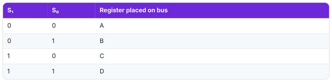
 A3 B3 C3 D3 A2 B2 C2 D2 A1 B1 C1 D1 A0 B0 C0 D0
 │ │ │ │ │ │ │ │ │ │ │ │ │ │ │ │
 ┌┴──┴──┴──┴┐ ┌┴──┴──┴──┴┐ ┌┴──┴──┴──┴┐ ┌┴──┴──┴──┴┐
 │ 4×1 MUX3 │ │ 4×1 MUX2 │ │ 4×1 MUX1 │ │ 4×1 MUX0 │ ◀── S1 S0 (shared)
 └────┬─────┘ └────┬─────┘ └────┬─────┘ └────┬─────┘
 │ bit3 │ bit2 │ bit1 │ bit0
 ═════╧══════════════╧══ 4-line common bus ════════╧════════
General rule: k registers of n bits → n multiplexers of size k × 1, with log₂k select lines. Example: 8 registers of 16 bits → 16 MUXes of 8 × 1, 3 select lines.
To transfer, e.g., R ← C : set S₁S₀ = 10 (C goes onto the bus) and enable the Load of register R.
How a common bus reduces connections (Q36): without a bus, 4 registers each needing a path to the other 3 need 4 × 3 = 12 sets of 4 wires = 48 wires plus selection logic at each register. With a bus: one set of 4 wires; each register connects once to the bus (output via the MUX, input via its load line). Adding a register just adds one MUX input instead of new paths to every register.
Three-state (tri-state) bus buffers
A three-state gate has three output states: 0, 1, and high impedance (behaves like an open circuit — disconnected).
Normal input A, control input C.
C = 1 → output Y = A; C = 0 → output is high-impedance (disconnected from the bus).
A common bus can be built with tri-state buffers instead of MUXes: each register’s bit drives the bus line through a buffer; a decoder enables exactly one buffer at a time, so only one register is ever connected to the bus. Advantage: easy to connect many sources.
Memory transfer
Read: DR ← M[AR] — the word at the address held in AR is transferred into the data register DR.
Write: M[AR] ← R1 — the contents of R1 are stored into memory at the address in AR.
1.7 Arithmetic micro-operations
| Symbolic | Description |
|---|---|
| R3 R1 + R2 ← | Contents of R1 plus R2 transferred to R3 |
| R3 R1 − R2 ← | R1 minus R2 (done as R1 + R2′ + 1) |
| R2 R2′ ← | Complement R2 (1’s complement) |
| R2 ← R2′ + 1 | 2’s complement of R2 (negate) |
| R3 ← R1 + R2′ + 1 | R1 + 2’s complement of R2 = subtraction |
| R1 ← R1 + 1 | Increment |
| R1 ← R1 − 1 | Decrement |
4-bit binary adder (Assignment Q14)
Made of 4 full adders connected in a chain: the carry out of each full adder is the carry in of the next (a ripple-carry adder). Inputs A₃…A₀, B₃…B₀, C₀; outputs S₃…S₀ and final carry C₄. An n-bit adder needs n full adders.
 B3 A3 B2 A2 B1 A1 B0 A0
 │ │ │ │ │ │ │ │
 ┌─┴──┴─┐ C3 ┌─┴──┴─┐ C2 ┌─┴──┴─┐ C1 ┌─┴──┴─┐
 C4◀─┤ FA │◀────┤ FA │◀────┤ FA │◀────┤ FA │◀── C0
 └──┬───┘ └──┬───┘ └──┬───┘ └──┬───┘
 S3 S2 S1 S0
Example: 1101 + 0111 → S = 0100, C₄ = 1 (13 + 7 = 20 = 1 0100 ✔).
4-bit adder-subtractor
Put an XOR gate on each B input, controlled by a mode input M, and connect M to C₀.
M = 0: B ⊕ 0 = B, C₀ = 0 → computes A + B.
M = 1: B ⊕ 1 = B′, C₀ = 1 → computes A + B′ + 1 = A − B.
Binary incrementer
Adds 1 to a register: a chain of half adders, with 1 fed into the first one. Example: 1101 + 1 = 1110.
4-bit arithmetic circuit (Assignment Q15)
One circuit that performs 8 arithmetic micro-operations. It uses a 4-bit parallel adder, and in front of each B input a 4 × 1 multiplexer that chooses what goes into the adder’s Y input, controlled by select lines S₁S₀; C_in is the carry input. Output D = A + Y + C_in.
| S₁ | S₀ | Y input | C_in = 0 | C_in = 1 |
|---|---|---|---|---|
| 0 | 0 | B | D = A + B (add) | D = A + B + 1 (add with carry) |
| 0 | 1 | B′ | D = A + B′ (subtract with borrow) | D = A + B′ + 1 = A − B (subtract) |
| 1 | 0 | 0 (all 0s) | D = A (transfer A) | D = A + 1 (increment) |
| 1 | 1 | 1 (all 1s) | D = A − 1 (decrement) | D = A (transfer A) |
Why does “Y = all 1s” decrement? All 1s = 1111 = −1 in 2’s complement, so A + 1111 = A − 1.
1.8 Logic micro-operations
Operate on each bit separately (bit-wise), no carries.
| on each bit separately (bit-wise), no | carries. |
|---|---|
| Micro-operation | Name |
| F ← A ∧ B | AND |
| F ← A ∨ B | OR |
| F ← A ⊕ B | XOR |
| F ← A′ | NOT (complement) |
| F ← (A ∧ B)′ | NAND |
| F ← (A ∨ B)′ | NOR |
| F ← (A ⊕ B)′ | XNOR |
There are 16 possible logic operations on two bits; the 4 basic ones (AND, OR, XOR, NOT) are implemented with gates and a 4 × 1 MUX.
Example: A = 1010, B = 1100 → AND = 1000, OR = 1110, XOR = 0110, NOT A = 0101, NAND = 0111, NOR = 0001, XNOR = 1001.
Applications (bit manipulation):
Selective set (set chosen bits to 1): A ← A ∨ B (B has 1s where bits should be set).
Selective clear / mask (clear chosen bits): A ← A ∧ B (B has 0s where bits should be cleared).
Selective complement (flip chosen bits): A ← A ⊕ B.
Clear a register: A ← A ⊕ A.
1.9 Shift micro-operations
Used for serial data transfer, multiplication/division by 2, bit manipulation.
| for serial data transfer, multiplication/division | by 2, bit manipulation. | |
|---|---|---|
| Type | What happens | Example on 10110010 |
| Logical shift left (shl) | All bits move left; 0 enters at the right; leftmost bit is lost | 01100100 |
| Logical shift right (shr) | All bits move right; 0 enters at the left | 01011001 |
| Circular shift left (cil) / rotate | Bits move left; the bit leaving the left re-enters at the right | 01100101 |
| Circular shift right (cir) | Bits move right; the bit leaving the right enters at the left | 01011001 |
| Arithmetic shift left (ashl) | Like logical left; multiplies a signed number by 2 (overflow if sign bit changes) | 01100100 (overflow!) |
| Arithmetic shift right (ashr) | Bits move right; sign bit is copied (stays the same) divides a → signed number by 2 | 11011001 |
Why arithmetic shift right copies the sign: 11110000 = −16. Logical shift right gives 01111000 = +120 (wrong). Arithmetic shift right gives 11111000 = −8 ✔ (−16 / 2).
Real-life uses (Assignment Q35): fast multiplication/division by powers of 2 in compilers (x × 8 → shift left 3), serial communication (UART sends bits one by one by shifting a register), graphics and image processing (extracting colour channels from a pixel), checksums/encryption (rotations), barcode scanners.
1.10 Arithmetic logic shift unit (ALSU)
Instead of separate units, one ALSU stage per bit combines:
the arithmetic circuit (8 operations), the logic circuit (4 operations), and a shifter (shr, shl), whose outputs go into a 4 × 1 MUX selected by S₃S₂: 00 → arithmetic, 01 → logic, 10 → shift right, 11 → shift left.
S₁S₀ (and C_in) choose the operation within the arithmetic/logic circuit.
| S₃ S₂ | S₁ S₀ | C_in | Operation |
|---|---|---|---|
| 00 | 00 | 0 | F = A (transfer) |
| 00 | 00 | 1 | F = A + 1 |
| 00 | 01 | 0 | F = A + B |
| 00 | 01 | 1 | F = A + B + 1 |
| 00 | 10 | 0 | F A = + B′ |
| 00 | 10 | 1 | F A B = − |
| 00 | 11 | 0 | F = A − 1 |
| 00 | 11 | 1 | F = A |
| 01 | 00 | × | F = A ∧ B |
| 01 | 01 | × | F = A ∨ B |
| 01 | 10 | × | F = A ⊕ B |
| 01 | 11 | × | F = A′ |
| 10 | ×× | × | F = shr A |
| 11 | ×× | × | F = shl A |
(14 operations total. Note this ordering of S₁S₀ in the ALSU table follows Mano’s ALSU figure; the earlier arithmetic-circuit table follows your notes’ version — learn whichever your teacher used; the idea is identical.)
The ALU (Assignment Q16) is the part of the CPU that carries out arithmetic (add, subtract, increment, decrement, multiply, divide), logic (AND, OR, XOR, NOT, compare) and shift operations; it also sets the status flags (carry, zero, sign, overflow). ALUs can be combinational (output depends only on current inputs — like the ALSU above) or sequential (uses registers and a control unit, e.g., for multiplication by repeated add-shift).
Part 1 — Check yourself
- 2’s complement of 01101000? 2. Range of 8-bit 2’s complement? 3. Write RTL for “if T₁ is 1, copy PC into AR”. 4. 8 registers, 32 bits each — how many MUXes, of what size, how many select lines? 5. Arithmetic shift right of 10010100?
Answers: 1) 10011000. 2) −128 to +127. 3) T₁: AR ← PC. 4) 32 MUXes of 8×1, 3 select lines. 5) 11001010.
Computer Arithmetic: Adders, Multiplication, Division, Floating Point
2.1 Half adder
In one line: a circuit that adds two bits and gives a sum and a carry.
| A | B | Sum | Carry |
|---|---|---|---|
| 0 | 0 | 0 | 0 |
| 0 | 1 | 1 | 0 |
| 1 | 0 | 1 | 0 |
| 1 | 1 | 0 | 1 |
Looking at the table: Sum is 1 when exactly one input is 1 → Sum = A ⊕ B (XOR). Carry is 1 only when both are 1 → Carry = A · B (AND). Circuit: one XOR gate + one AND gate.
Limitation: it can’t accept a carry coming from a previous column, so it can only add the least significant bits.
2.2 Full adder
In one line: adds three bits — A, B and an incoming carry C — giving Sum and Carry-out.
| A | B | C | Sum | Cout |
|---|---|---|---|---|
| 0 | 0 | 0 | 0 | 0 |
| 0 | 0 | 1 | 1 | 0 |
| 0 | 1 | 0 | 1 | 0 |
| 0 | 1 | 1 | 0 | 1 |
| 1 | 0 | 0 | 1 | 0 |
| 1 | 0 | 1 | 0 | 1 |
| 1 | 1 | 0 | 0 | 1 |
| 1 | 1 | 1 | 1 | 1 |
Sum = A ⊕ B ⊕ C (1 when an odd number of inputs are 1). Cout = AB + BC + AC (1 when at least two inputs are 1).
Derivation of Cout (from your notes): Cout = A′BC + AB′C + ABC′ + ABC. Add ABC twice more (allowed since x + x = x) and group: = BC(A′ + A) + AC(B′ + B) + AB(C′ + C) = BC + AC + AB.
A full adder can be built from two half adders and an OR gate: first HA adds A and B; second HA adds that sum to C; OR the two carries.
2.3 n-bit binary parallel adder (ripple-carry adder)
Adds two n-bit numbers using n full adders in cascade — the carry output of each is connected to the carry input of the next (diagram in Part 1.7).
 C3 C2 C1 C0=0 ← carries
 A3 A2 A1 A0
 + B3 B2 B1 B0
 ──────────────
 C4 S3 S2 S1 S0
The problem — carry propagation delay: the sum bit S₃ can’t be correct until the carry has rippled through every previous stage. Each stage adds a gate delay, so an n-bit adder’s delay grows with n. For 64-bit numbers this is too slow. Solution ↓
2.4 Carry look-ahead adder (fast adder)
In one line: compute all carries at the same time directly from the inputs, instead of waiting for them to ripple.
Two helper signals for each bit position i:
Carry generate: 𝐺𝑖= 𝐴𝑖𝐵𝑖 — this position creates a carry by itself (both bits 1).
Carry propagate: 𝑃𝑖= 𝐴𝑖⊕𝐵𝑖 — this position passes on an incoming carry (exactly one bit is 1).
Then: Sᵢ = Pᵢ ⊕ Cᵢ and Cᵢ₊₁ = Gᵢ + PᵢCᵢ (“a carry comes out if this stage generates one, or propagates the incoming one”).
Now expand each carry so it depends only on G’s, P’s and C₀:
C₁ = G₀ + P₀C₀
C₂ = G₁ + P₁C₁ = G₁ + P₁G₀ + P₁P₀C₀
C₃ = G₂ + P₂C₂ = G₂ + P₂G₁ + P₂P₁G₀ + P₂P₁P₀C₀
C₄ = G₃ + P₃G₂ + P₃P₂G₁ + P₃P₂P₁G₀ + P₃P₂P₁P₀C₀
Every carry is now a two-level AND-OR expression of the inputs → all carries appear after the same small, fixed delay, no matter the position. The 4-bit CLA block diagram: P/G generator → carry look-ahead generator → XOR gates for the sums.
| look-ahead generator → XOR gates | for the sums. |
|---|---|
| Ripple-carry adder | Carry look-ahead adder |
| Carry passes stage by stage | All carries computed in parallel |
| Delay grows linearly with n | Delay roughly constant (for a block) |
| Simple, cheap | More gates, complex for large n |
2.5 Addition and subtraction of signed-magnitude numbers (PPT Unit 7)
When numbers are stored in signed magnitude (sign bit + magnitude), the hardware must look at the signs:
Rule for A ± B (As, Bs = sign bits):
Add operation with equal signs, or subtract with different signs → add the magnitudes; result takes the sign of A. (If there is a carry out → overflow.)
Add with different signs, or subtract with equal signs → subtract the magnitudes: compute A + B′ + 1.
If end carry E = 1 → A ≥ B, result is correct, sign = As.
If E = 0 → A < B, take the 2’s complement of the result and flip the sign. (If result is 0, make the sign + .)
Hardware: registers A and B with sign flip-flops As and Bs, a parallel adder, a complementer (XOR with mode M), the end-carry flip-flop E, and an AVF (add overflow flip-flop).
2.6 Multiplication
Unsigned multiplication — paper method
Multiply by each bit of the multiplier and add shifted partial products:
 1011 (11)
 × 1101 (13)
 ──────
 1011
 0000
 1011
 1011
 ────────
 10001111 (143) ✔
Booth’s multiplication algorithm (signed 2’s complement numbers)
Why Booth? Handles negative numbers directly in 2’s complement and can skip over strings of 1s (fewer additions).
Registers: A (accumulator, starts at 0), Q (multiplier), Q₋₁ (one extra bit to the right of Q, starts at 0), M (multiplicand). Count = number of bits n.
Rule — look at the pair (Q₀, Q₋₁):
| — look at the | pair (Q₀, Q₋₁): |
|---|---|
| Q₀ Q₋₁ | Action |
| 0 0 | no operation (middle of a string of 0s) |
| 1 1 | no operation (middle of a string of 1s) |
| 1 0 | A A − M (start of a string of 1s) ← |
| 0 1 | A ← A + M (end of a string of 1s) |
After the action, arithmetic shift right A, Q, Q₋₁ together (A’s sign bit is copied), and decrement count. Repeat n times. Product = A:Q.
 ┌───────┐
 │ START │ A ← 0, Q₋₁ ← 0, M ← multiplicand, Q ← multiplier, count ← n
 └───┬───┘
 ▼
 ┌──────────────┐ 10 ┌──────────┐
 │ Check Q₀Q₋₁ │─────────────▶│ A ← A − M │──┐
 └──────┬───────┘ 01 └──────────┘ │
 │ ────────────────────▶ A ← A + M ───┤
 │ 00 or 11 │
 ▼◀────────────────────────────────────┘
 Arithmetic shift right A, Q, Q₋₁ ; count ← count − 1
 │
 count = 0 ? ── No ──▶ back to Check
 │ Yes
 ▼
 END (product in A:Q)
Worked example: 7 × (−3) using 4 bits. M = 7 = 0111, −M = 1001 (2’s complement), Q = −3 = 1101.
| Step | Q₀Q₋₁ | Action | A | Q | Q₋₁ |
|---|---|---|---|---|---|
| Initial | 0000 | 1101 | 0 | ||
| 1 | 10 | A ← A − M ASHR | 1001 1100 | 1101 1110 | 0 1 |
| 2 | 01 | A ← A + M ASHR | 0011 0001 | 1110 1111 | 1 0 |
| 3 | 10 | A ← A − M ASHR | 1010 1101 | 1111 0111 | 0 1 |
| 4 | 11 | none ASHR | 1101 1110 | 0111 1011 | 1 1 |
Product A:Q = 1110 1011. Sign bit 1 → negative. 2’s complement = 0001 0101 = 21 → −21 ✔ (7 × −3 = −21).
How the ASHR works in step 1: A:Q:Q₋₁ = 1001 1101 0 → shift everything right by one, copy A’s sign bit (1) into the new leftmost position → 1100 1110 1.
Array multiplier (combinational)
Multiplication done entirely with gates (no repeated steps): AND gates form all partial-product bits aᵢbⱼ, and adders add them. For 2 × 2 bits: product bits C₀ = a₀b₀; C₁ = a₁b₀ + a₀b₁ (half adder); C₂, C₃ from a second half adder. A j × k bit array multiplier needs j × k AND gates and (j − 1) k-bit adders to produce a (j + k)-bit product. A 4 × 3 multiplier: 12 AND gates and two 4-bit adders. ✔ Very fast. ✘ Lots of hardware.
2.7 Division — restoring algorithm (unsigned integers)
Registers: A (remainder, n+1 bits, starts 0), Q (dividend, becomes the quotient), M (divisor). Repeat n times:
-
Shift left A and Q together (as one register A:Q).
-
A ← A − M.
-
If A is negative (sign bit 1): set Q₀ = 0 and restore A ← A + M. If A is positive or zero: set Q₀ = 1. At the end, Q = quotient, A = remainder.
Worked example: 11 ÷ 3 (n = 4). Q = 1011, M = 00011, −M = 11101.
| Step | Operation | A | Q |
|---|---|---|---|
| Init | 00000 | 1011 | |
| 1 | Shift left A:Q A ← A − M Q₀ = 0, restore A | 00001 11110 (neg) 00001 | 011_ 0110 |
| 2 | Shift left A − M Q₀ = 0, restore | 00010 11111 (neg) 00010 | 110_ 1100 |
| 3 | Shift left A − M Q₀ = 1 | 00101 00010 (pos) 00010 | 100_ 1001 |
| 4 | Shift left A − M Q₀ = 1 | 00101 00010 (pos) 00010 | 001_ 0011 |
Quotient Q = 0011 = 3, Remainder A = 00010 = 2 ✔ (11 = 3 × 3 + 2).
(Non-restoring division avoids the restore step: if A is negative, in the next step add M instead of subtracting after the shift; a final correction is needed if the remainder is negative.)
2.8 Floating-point arithmetic
Addition and subtraction — four phases
-
Check for zero — if one operand is 0, the result is the other.
-
Align the significands (mantissas) — make the exponents equal by shifting the mantissa of the smaller number to the right and increasing its exponent (shifting the smaller number loses the least important bits).
-
Add or subtract the significands.
-
Normalize the result — shift the mantissa left until the first digit is non-zero (decreasing the exponent), or right by one if the addition overflowed; then round.
Example (decimal): X = 0.3 × 10², Y = 0.2 × 10³.
Align: X = 0.03 × 10³.
X + Y = (0.03 + 0.2) × 10³ = 0.23 × 10³ = 230 ✔
X − Y = (0.03 − 0.2) × 10³ = −0.17 × 10³ = −170 ✔
Multiplication
-
Check for zero (if either is 0 → result 0).
-
Add the exponents (with biased exponents, subtract one bias: E = E₁ + E₂ − bias).
-
Multiply the significands.
-
Normalize and round. Check exponent overflow/underflow.
Division
-
Check for zero (divisor 0 → error/infinity; dividend 0 → 0).
-
Subtract the exponents (add the bias back).
-
Divide the significands.
-
Normalize and round.
Problems that can occur
Exponent overflow: a positive exponent exceeds the maximum → +∞ or −∞.
Exponent underflow: a negative exponent is below the minimum → number too small → reported as 0.
Significand underflow: during alignment, digits shift off the right end → rounding needed. Significand overflow: adding two significands of the same sign produces a carry → shift right and increment the exponent (realignment).
2.9 Decimal arithmetic unit (BCD adder)
BCD (Binary Coded Decimal): each decimal digit is stored as 4 bits: 59 → 0101 1001.
Problem: adding two BCD digits in binary may give a result > 9 (invalid BCD codes 1010–1111) or a carry. Rule: if the 4-bit binary sum is greater than 9, or produces a carry, add 6 (0110) to correct it, and send a carry to the next digit.
Example: 8 + 7 = 1000 + 0111 = 1111 (15 > 9) → 1111 + 0110 = 1 0101 → digit 5, carry 1 → 15 ✔.
BCD adder circuit: a 4-bit binary adder, a correction detector C = K + Z₈Z₄ + Z₈Z₂ (K = carry out, Z = sum bits), and a second 4-bit adder that adds 0110 when C = 1.
Part 2 — Check yourself
- Write Sum and Carry of a full adder. 2. What are Pᵢ and Gᵢ? 3. In Booth’s, what do you do for Q₀Q₋₁ = 10? 4. 9 + 5 in BCD? Answers: 1) A⊕B⊕C; AB + BC + AC. 2) Pᵢ = Aᵢ ⊕ Bᵢ, Gᵢ = AᵢBᵢ. 3) A ← A − M, then ASHR. 4) 1001 + 0101 = 1110 > 9 → + 0110 = 1 0100 → 14.
Basic Computer Organization and Design (Mano’s Basic Computer)
Your Unit-2 PPT studies a small, complete imaginary computer designed by M. Morris Mano, the “basic computer”. Learn it as a working model — once you understand it, every real CPU makes sense.
3.1 Instruction codes
A program is a set of instructions; an instruction is a binary code telling the computer to perform a specific operation.
An instruction code is a group of bits divided into parts. The most basic part is the operation code (opcode) — the bits that say which operation (ADD, LOAD, …).
With n opcode bits, there can be up to 2ⁿ distinct operations. (4-bit opcode → 16 operations.) The other part gives the address of the operand (where the data is).
Stored program organization (Assignment Q5)
In one line: both the program instructions and the data are stored in the same memory; the CPU reads instructions one by one from memory and executes them.
The basic computer’s memory: 4096 words × 16 bits. Since 4096 = 2¹², an address needs 12 bits. Each 16-bit instruction is split:
 15 12 11 0
 ┌──────────┬────────────────────────────┐
 │ Opcode │ Address │ Instruction format
 │ 4 bits │ 12 bits │
 └──────────┴────────────────────────────┘
 15 0
 ┌───────────────────────────────────────┐
 │ Binary operand (16 bits) │ Data word
 └───────────────────────────────────────┘
 Memory 4096 × 16 Processor
 ┌─────────────────────┐ ┌──────────────────────┐
 │ Instructions │ │ Accumulator (AC) │
 │ (program) │────────▶│ — the only │
 ├─────────────────────┤ │ processor register│
 │ Operands (data) │────────▶│ │
 └─────────────────────┘ └──────────────────────┘
Opcode 4 bits → up to 16 operations.
The single processor register is the Accumulator (AC). An instruction like ADD reads the operand from memory and adds it to AC.
Direct and indirect address
The basic computer instruction has one more field: bit 15 = I (addressing mode bit).
 15 14 12 11 0
 ┌──┬───────┬──────────────┐
 │ I│Opcode │ Address │
 └──┴───────┴──────────────┘
I = 0 → direct address: the address field is the address of the operand. “ADD 457” → operand is in memory word 457.
I = 1 → indirect address: the address field holds the address of a memory word which contains the address of the operand. “ADD I 300” where M[300] = 1350 → operand is in word 1350.
Effective address (EA) = the actual address of the operand.
Analogy: direct = “the book is on shelf 457”. Indirect = “go to shelf 300; there’s a note saying the book is on shelf 1350”.
3.2 Computer registers
| Symbol | Bits | Name | Function |
|---|---|---|---|
| DR | 16 | Data register | Holds the memory operand |
| AR | 12 | Address register | Holds the address for memory |
| AC | 16 | Accumulator | Processor register (results) |
| IR | 16 | Instruction register | Holds the instruction code |
| PC | 12 | Program counter | Holds the address of the next instruction |
| TR | 16 | Temporary register | Holds temporary data |
| INPR | 8 | Input register | Holds the input character |
| OUTR | 8 | Output register | Holds the output character |
Why are AR and PC 12 bits? Because they hold addresses, and an address is 12 bits (4096 words). DR, AC, IR, TR hold words (16 bits). INPR and OUTR hold one 8-bit character.
3.3 Common bus system of the basic computer
The 8 registers + memory are connected by a 16-bit common bus. Three select lines S₂S₁S₀ choose which register’s output goes onto the bus:
| which register’s | output goes onto the bus: | |
|---|---|---|
| S₂S₁S₀ | Decimal | Register on bus |
| 000 | 0 | (none) |
| 001 | 1 | AR |
| 010 | 2 | PC |
| 011 | 3 | DR |
| 100 | 4 | AC |
| 101 | 5 | IR |
| 110 | 6 | TR |
| 111 | 7 | Memory |
 ┌──────── 16-bit common bus ─────────────────────────────┐
 S2 S1 S0 │ │
 ─────────┤ Memory unit 4096×16 (7) ◀── Address ── AR │
 │ AR (1) LD INR CLR │
 │ PC (2) LD INR CLR │
 │ DR (3) LD INR CLR │
 │ Adder & logic ── E │
 │ AC (4) LD INR CLR INPR ──▶ adder │
 │ IR (5) LD │
 │ TR (6) LD INR CLR │
 │ OUTR LD │
 └─────────────────────────────────────────────────────────┘
 Clock
Each register has control inputs: LD (load from bus), INR (increment), CLR (clear).
When a register is loaded, it takes its data from the bus. The register whose LD is enabled receives the bus contents at the next clock pulse.
Memory gets its address always from AR. A memory read puts the word on the bus (S = 111); a write takes data from the bus.
AC is loaded only through the adder & logic circuit (inputs: AC, DR, INPR). E is the extended carry flip-flop.
Two micro-operations can happen in one clock cycle if they don’t both need the bus, e.g. DR ← AC, AC ← DR (AC goes onto the bus to DR, while DR goes through the adder-logic to AC).
3.4 Computer instructions
Three instruction formats (16 bits each):
Memory-reference: 15 | 14 13 12 | 11 ............ 0
 I | opcode | address opcode 000–110
Register-reference: 0 1 1 1 | register operation (opcode 111, I = 0) → hex 7xxx
Input-output: 1 1 1 1 | I/O operation (opcode 111, I = 1) → hex Fxxx
The control decodes bits 12–14: if they are 111, the instruction is not memory-reference — then bit 15 tells register (0) or I/O (1). The remaining 12 bits specify the operation.
Instruction set (memorise the names, the hex codes help in programs)
Memory-reference instructions (hex: direct I=0 / indirect I=1)
| Symbol | Direct | Indirect | Description |
|---|---|---|---|
| AND | 0xxx | 8xxx | AND memory word to AC |
| ADD | 1xxx | 9xxx | Add memory word to AC (carry → E) |
| LDA | 2xxx | Axxx | Load memory word to AC |
| STA | 3xxx | Bxxx | Store content of AC in memory |
| BUN | 4xxx | Cxxx | Branch unconditionally |
| BSA | 5xxx | Dxxx | Branch and save return address |
| ISZ | 6xxx | Exxx | Increment and skip if zero |
Register-reference instructions (7xxx)
| instructions | (7xxx) | |
|---|---|---|
| Symbol | Hex | Description |
| CLA | 7800 | Clear AC |
| CLE | 7400 | Clear E |
| CMA | 7200 | Complement AC |
| CME | 7100 | Complement E |
| CIR | 7080 | Circulate right AC and E |
| CIL | 7040 | Circulate left AC and E |
| INC | 7020 | Increment AC |
| SPA | 7010 | Skip next instruction if AC positive |
| SNA | 7008 | Skip if AC negative |
| SZA | 7004 | Skip if AC zero |
| SZE | 7002 | Skip if E zero |
| HLT | 7001 | Halt computer |
Input-output instructions (Fxxx)
| instructions | (Fxxx) | |
|---|---|---|
| Symbol | Hex | Description |
| INP | F800 | Input character to AC |
| OUT | F400 | Output character from AC |
| SKI | F200 | Skip on input flag |
| SKO | F100 | Skip on output flag |
| ION | F080 | Interrupt on |
| IOF | F040 | Interrupt off |
Instruction set completeness: a computer’s instruction set is complete if it has instructions for (1) arithmetic, logical and shift operations, (2) moving data between memory and registers, (3) program control (branches) and status checks, (4) input and output. The basic computer has all four (e.g., subtraction is done with CMA, INC, ADD).
3.5 Timing and control
The control unit generates the control signals at the right times. Two kinds of control
organization:
Hardwired control — logic built from gates, flip-flops, decoders. ✔ Fast. ✘ Hard to modify. Microprogrammed control — control information stored in a control memory (Part 5). ✔ Easy to modify. ✘ Slower.
Hardwired control unit of the basic computer:
 Instruction register IR
 ┌──┬──────────┬───────────────────┐
 │15│ 14 13 12 │ 11 ......... 0 │
 └┬─┴────┬─────┴─────────┬─────────┘
 │ 3×8 decoder │ (bits 0–11 go directly to control logic)
 │ D0 … D7 │
 ▼ ▼ ▼
 ┌─────────────────────────────────┐
 │ Control logic gates │──▶ control outputs (LD, INR, CLR, S2S1S0, memory R/W …)
 └─────────────────────────────────┘
 ▲ T0 … T15
 ┌──────┴────────┐ 4×16 decoder
 │ Sequence │──▶
 │ counter (SC) │ INR, CLR ← from control logic
 └───────────────┘
 ▲ clock
The sequence counter (SC) is a 4-bit counter, incremented every clock pulse. Its output is decoded into 16 timing signals T₀ … T₁₅. At T₀ the first step happens, at T₁ the next, and so on.
The opcode bits 12–14 are decoded into D₀ … D₇ (D₀ = AND, D₁ = ADD, …, D₇ = register/I-O). Bit 15 goes to flip-flop I.
The control logic combines Tᵢ, Dⱼ and I to produce every control signal. SC is cleared (SC ←
- at the end of each instruction, so the next instruction starts at T₀.
Example: D₃T₄: SC ← 0 means “if the decoded opcode is D₃ and the time is T₄, clear the sequence counter”.
3.6 The instruction cycle
Each instruction is processed in phases:
-
Fetch the instruction from memory.
-
Decode it.
-
Read the effective address from memory if the instruction has an indirect address.
-
Execute it.
Then go back to step 1 for the next instruction (unless HLT).
Fetch and decode (in RTL — learn these three lines exactly)
T0: AR ← PC (put address of instruction in AR)
T1: IR ← M[AR], PC ← PC + 1 (read instruction; point PC to next one)
T2: D0…D7 ← Decode IR(12–14), AR ← IR(0–11), I ← IR(15)
Why does T₀ need its own step? Memory always takes its address from AR, so PC must first be copied to AR. At T₁, memory (S = 111) puts the instruction on the bus and IR loads it; at the same time PC is incremented (INR, no bus needed).
Determining the type of instruction (flowchart)
 Start: SC ← 0
 │
 T0 AR ← PC
 T1 IR ← M[AR], PC ← PC + 1
 T2 Decode, AR ← IR(0–11), I ← IR(15)
 │
 D7 = 1 ? (opcode 111)
 / \
 No (memory-ref) Yes (register or I/O)
 │ │
 I = 1 ? I = 1 ?
 / \ / \
 Yes No Yes No
 T3: AR ← M[AR] T3: nothing T3: execute I/O T3: execute register-ref
 (indirect) (direct) instruction instruction
 \ / SC ← 0 SC ← 0
 T4: execute memory-reference instruction … SC ← 0
Register-reference instructions (executed at T₃)
r = D₇ I′ T₃ (common condition), Bᵢ = bit i of IR:
| Condition | Micro-operation | |
|---|---|---|
| CLA | rB₁₁ | AC ← 0 |
| CLE | rB₁₀ | E ← 0 |
| CMA | rB₉ | AC ← AC′ |
| CME | rB₈ | E ← E′ |
| CIR | rB₇ | AC E ← shr AC, AC(15) ← E, ← AC(0) |
| CIL | rB₆ | AC E ← shl AC, AC(0) ← E, ← AC(15) |
| INC | rB₅ | AC AC + 1 ← |
| SPA | rB₄ | If AC(15) = 0 then PC PC + 1 ← |
| SNA | rB₃ | If AC(15) = 1 then PC PC + 1 ← |
| SZA | rB₂ | If AC = 0 then PC ← PC + 1 |
| SZE | rB₁ | If E = 0 then PC ← PC + 1 |
| HLT | rB₀ | S ← 0 (stop) |
(All end with SC ← 0.) Skip works by incrementing PC once more, jumping over the next instruction.
3.7 Memory-reference instructions (executed from T₄)
The effective address is in AR (after T₂ for direct, T₃ for indirect).
| effective | address is in | AR (after T₂ for direct, T₃ for indirect). |
|---|---|---|
| Symbol | Decoder | Symbolic description |
| AND | D₀ | AC ← AC ∧ M[AR] |
| ADD | D₁ | AC ← AC + M[AR], E ← Cout |
| LDA | D₂ | AC ← M[AR] |
| STA | D₃ | AC M[AR] ← |
| BUN | D₄ | PC AR ← |
| BSA | D₅ | M[AR] PC, PC AR + 1 ← ← |
| ISZ | D₆ | M[AR] M[AR] + 1; if M[AR] + 1 = 0 then PC PC + 1 ← ← |
Micro-operation sequences (why each takes several clocks: the operand must first be brought into DR, because the adder takes its input from DR, not directly from memory):
AND: D0T4: DR ← M[AR]
 D0T5: AC ← AC ∧ DR, SC ← 0
ADD: D1T4: DR ← M[AR]
 D1T5: AC ← AC + DR, E ← Cout, SC ← 0
LDA: D2T4: DR ← M[AR]
 D2T5: AC ← DR, SC ← 0
STA: D3T4: M[AR] ← AC, SC ← 0
BUN: D4T4: PC ← AR, SC ← 0
BSA: D5T4: M[AR] ← PC, AR ← AR + 1
 D5T5: PC ← AR, SC ← 0
ISZ: D6T4: DR ← M[AR]
 D6T5: DR ← DR + 1
 D6T6: M[AR] ← DR, if (DR = 0) then (PC ← PC + 1), SC ← 0
BSA (Branch and Save return Address) is how subroutines are called. Example: at address 20 is “BSA 135”. PC = 21 after fetch. BSA stores 21 into M[135] and sets PC = 136 (subroutine starts at 136). At the end of the subroutine, “BUN 135 I” (indirect) jumps to the address stored at 135, i.e., back to 21.
ISZ is used for loops: store −N in a counter; ISZ increments it each pass; when it reaches 0, the next instruction (the branch back) is skipped → loop ends.
3.8 Input-output and interrupt
I/O configuration
 Keyboard ──▶ Receiver interface ──▶ INPR (8 bits) ──▶ AC
 FGI (input flag)
 Printer ◀── Transmitter interface ◀── OUTR (8 bits) ◀── AC
 FGO (output flag)
FGI = 1 when a new character is in INPR (ready to be read). The computer reads it and clears FGI.
FGO = 1 when the printer is ready to accept a new character. The computer puts a character in OUTR and clears FGO.
I/O instructions (p = D₇IT₃): INP: AC(0–7) ← INPR, FGI ← 0; OUT: OUTR ← AC(0–7), FGO ← 0; SKI: if FGI = 1 skip; SKO: if FGO = 1 skip; ION: IEN ← 1; IOF: IEN ← 0.
Why interrupts? (program-controlled vs interrupt)
Program-controlled I/O: the CPU keeps checking the flag in a loop (“SKI, BUN back”) — it wastes time because the CPU is thousands of times faster than a keyboard. Interrupt-driven I/O: the CPU does useful work; when a device is ready, the device interrupts the CPU, which then services it.
Interrupt cycle
IEN (interrupt enable flip-flop) — set by ION, cleared by IOF.
R (interrupt flip-flop) — set when an interrupt is pending: T₀′T₁′T₂′(IEN)(FGI + FGO): R ← 1 . After finishing the current instruction, instead of a normal fetch, if R = 1 the computer goes through the interrupt cycle:
RT0: AR ← 0, TR ← PC (save return address in TR)
RT1: M[AR] ← TR, PC ← 0 (store return address in location 0)
RT2: PC ← PC + 1, IEN ← 0, R ← 0, SC ← 0 (go to location 1; disable further interrupts)
Location 1 holds a branch to the interrupt service routine, which ends by turning interrupts back on (ION) and returning with “BUN 0 I”.
 Instruction cycle ──── R = 0 ────▶ Fetch & decode → Execute
 │
 R = 1
 ▼
 Interrupt cycle: M[0] ← PC, PC ← 1, IEN ← 0, R ← 0
3.9 Complete computer description and design of the accumulator logic
The complete description = all the control functions and micro-operations above (fetch, decode, indirect, interrupt, memory-reference, register-reference, I/O) in one table. From it, the designer derives the logic for each register’s LD/INR/CLR inputs, the bus select lines and memory read/write.
Design of accumulator logic: collect every statement that changes AC:
D0T5: AC ← AC ∧ DR (AND)
D1T5: AC ← AC + DR (ADD)
D2T5: AC ← DR (LDA)
pB11: AC(0–7) ← INPR (INP)
rB9: AC ← AC′ (CMA)
rB7: AC ← shr AC (CIR)
rB6: AC ← shl AC (CIL)
rB11: AC ← 0 (CLA)
rB5: AC ← AC + 1 (INC)
So AC’s LD = OR of (D₀T₅, D₁T₅, D₂T₅, pB₁₁, rB₉, rB₇, rB₆); CLR = rB₁₁; INR = rB₅. The adder-and- logic circuit has 16 identical stages, each choosing AND / ADD / DR transfer / INPR /
complement / shift for its bit.
Part 3 — Check yourself
- Why is AR 12 bits? 2. Write the fetch micro-operations. 3. M[300] = 1350, instruction “ADD I 300”. What is the effective address? 4. What does BSA store and where?
Answers: 1) Memory has 4096 = 2¹² words. 2) T₀: AR ← PC; T₁: IR ← M[AR], PC ← PC + 1; T₂: decode, AR ← IR(0–11), I ← IR(15). 3) 1350. 4) The return address (PC) into M[AR] — the first word of the subroutine.
Programming the Basic Computer
4.1 Machine language and assembly language
Categories of programs:
-
Binary code — instructions and data written as 0s and 1s exactly as stored in memory.
-
Octal or hexadecimal code — the same, written in octal/hex for convenience.
-
Symbolic code (assembly language) — each instruction written with symbols (mnemonics) like ADD, LDA; translated by an assembler into binary.
-
High-level language — C, Java; translated by a compiler.
Machine language = categories 1 and 2 (directly executable). Assembly language = one symbolic line per machine instruction.
Example — add two numbers, all four ways:
| — add | two numbers, all four ways: | ||
|---|---|---|---|
| Location | Binary | Hex | Symbolic |
| 000 | 0010 0000 0000 0100 | 2004 | LDA 004 |
| 001 | 0001 0000 0000 0101 | 1005 | ADD 005 |
| 002 | 0011 0000 0000 0110 | 3006 | STA 006 |
| 003 | 0111 0000 0000 0001 | 7001 | HLT |
| 004 | 0000 0000 0101 0011 | 0053 | first operand |
| 005 | 1111 1111 1110 1001 | FFE9 | second operand (−23) |
| 006 | 0000 0000 0000 0000 | 0000 | sum store here |
4.2 Assembly language rules
Each line has three fields: Label | Instruction | Comment (after / ).
Label — symbolic address (up to 3 characters, ends with a comma).
Instruction — a memory-reference instruction (MRI) with an address (+ optional I for indirect), a register-reference or I/O instruction (no address), or a pseudo-instruction. Pseudo-instructions — directions to the assembler, not machine instructions:
| Pseudo-instruction | Meaning |
|---|---|
| ORG N | The next line is placed at memory location N (hex) |
| END | End of the program |
| DEC N | Store the decimal number N (converted to binary) |
| HEX N | Store the hex number N |
Example: subtract two numbers (DIF = MIN − SUB)
 ORG 100 / origin of program is location 100
 LDA SUB / load subtrahend to AC
 CMA / complement AC
 INC / increment AC → AC = −SUB (2's complement)
 ADD MIN / add minuend to AC
 STA DIF / store difference
 HLT / halt
MIN, DEC 83 / minuend
SUB, DEC −23 / subtrahend
DIF, HEX 0 / difference stored here
 END
Result: 83 − (−23) = 106.
4.3 The assembler
An assembler translates the symbolic program into binary. It scans the program twice (two- pass assembler):
First pass — build the address symbol table.
A location counter (LC) keeps track of the memory address of each line. ORG sets LC; each instruction or data line increments LC by 1.
When a label is found, store (label, current LC) in the address-symbol table. For the program above: MIN = 106, SUB = 107, DIF = 108.
Stop at END.
Second pass — translate.
Using the tables: pseudo-instruction table (ORG, END, DEC, HEX), MRI table (7 symbols with opcodes), non-MRI table (18 register/I/O instructions with their hex codes), and the address- symbol table from pass 1.
Each MRI → opcode bits + address bits (from the symbol table) + I bit; each non-MRI → its 16-bit code; DEC/HEX → binary number. Errors (e.g., unknown symbol) are reported.
Why two passes? A label may be used before it is defined (LDA SUB appears before SUB’s line), so its address isn’t known yet in a single pass.
4.4 Program loops
A loop repeats a sequence of instructions. Example: sum of 100 numbers stored from location 150.
 ORG 100
 LDA ADS / load first address of operands
 STA PTR / store in pointer
 LDA NBR / load −100
 STA CTR / store in counter
 CLA / clear AC
LOP, ADD PTR I / add an operand to AC (indirect through pointer)
 ISZ PTR / increment pointer
 ISZ CTR / increment counter; skip next when it becomes 0
 BUN LOP / repeat loop
 STA SUM / store sum
 HLT
ADS, HEX 150 / first address of operands
PTR, HEX 0 / pointer
NBR, DEC −100 / −100 initial counter value
CTR, HEX 0 / counter
SUM, HEX 0 / sum stored here
 ORG 150
 DEC 75 / first operand
 … / 100 operands
 DEC 23 / last operand
 END
Key ideas: a pointer (PTR) with indirect addressing walks through the array; a counter (CTR) starting at −100 is incremented by ISZ; when it reaches 0, ISZ skips the BUN and the loop ends.
4.5 Programming arithmetic and logic operations
The basic computer has no multiply instruction, so multiplication is done in software by shift- and-add:
Check each bit of the multiplier (shift it right with CIR into E).
If the bit is 1, add the (shifted) multiplicand to the partial product.
Shift the multiplicand left (CIL) each time.
Repeat for all bits (counter with ISZ).
Logic operations: AND is available; OR is made using De Morgan: A ∨ B = (A′ ∧ B′)′ → CMA, AND with complemented B, CMA. Shift operations use CIL/CIR with E cleared first (CLE) for a logical shift.
Double-precision addition (32-bit numbers in two words each): add the low halves, the carry goes to E; then add the high halves plus E (moved into AC with CIL).
4.6 Subroutines
A subroutine is a set of instructions that can be used many times from different places in a program.
Call: BSA SUB — saves the return address in the first word of the subroutine and jumps to the second word.
Return: BUN SUB I — indirect jump through the saved return address.
Parameters can be passed in AC, or in the memory words right after the BSA instruction (the subroutine reads them through the saved return address and increments it to skip them).
 ORG 100
100 LDA X / load X
101 BSA SH4 / call subroutine (shift left 4 times)
102 STA X / result returns here
…
SH4, HEX 0 / return address stored here
 CIL / circulate left 4 times
 CIL
 CIL
 CIL
 AND MSK / clear the 4 low bits
 BUN SH4 I / return to caller
MSK, HEX FFF0
4.7 Input-output programming
CIF, SKI / check input flag
 BUN CIF / flag = 0 → keep waiting
 INP / flag = 1 → input character
 OUT / echo it back
 STA CHR / store character
 HLT
CHR, — / store character here
Similarly for output: COF, SKO / BUN COF / LDA CHR / OUT . Character manipulation: two 8-bit characters can be packed into one 16-bit word (input first, shift left 8 times with CIL, input second). Interrupt-driven I/O programs save AC and E at the start of the service routine, check SKI/SKO to find which device interrupted, service it, restore AC and E, turn ION on, and return with BUN 0 I.
Part 4 — Check yourself
- What does ORG 100 do? 2. Why does the assembler need two passes? 3. How does the loop counter work with ISZ? 4. How is a subroutine called and how does it return? Answers: 1) Places the next instruction at location 100. 2) Labels may be used before they’re defined. 3) Start at −N; ISZ adds 1; at 0 it skips the branch. 4) BSA saves the return address and jumps; BUN … I returns.
Microprogrammed Control
5.1 The idea
The control unit’s job is to produce control signals (e.g., “load AC”, “increment PC”, “read memory”) in the right order. There are two ways to build it:
Hardwired control: the control signals are produced by fixed logic circuits (gates, flip-flops, decoders, the sequence counter — Part 3.5). Microprogrammed control: the control signals for each step are stored as binary words in a special memory — the control memory. To execute an instruction, the control unit simply reads a sequence of these words, one per clock pulse, and sends their bits out as control signals.
Analogy: a hardwired control unit is a music box — the tune is built into the pins and can’t be changed. A microprogrammed control unit is a piano player reading sheet music — change the sheet, and it plays a different tune.
Vocabulary (learn these definitions exactly)
| Term | Meaning |
|---|---|
| Control word | A string of 1s and 0s where each bit (or group) represents a control signal |
| Micro-operation | An elementary operation done in one clock pulse (e.g., AC ← AC + DR) |
| Microinstruction | A control word stored in control memory; specifies one or more micro-operations (+ info on what comes next) |
| Microprogram | A sequence of microinstructions (e.g., the routine that executes ADD) |
| Microcode | The microinstructions collectively — the “firmware” of the CPU |
| Control memory | The memory holding the microprogram — usually ROM (contents fixed); writable control memory if it can be changed |
| Control address register (CAR) | Holds the address of the next microinstruction to read |
| Control data register (CDR) | (optional) Holds the microinstruction just read — also called the pipeline register |
| Sequencer (next-address generator) | to CAR Circuit that decides the next address load into |
5.2 Microprogrammed control organization
 External input
 (instruction bits, ┌─────────────┐ ┌─────────┐ ┌──────────────┐ ┌──────────┐
 status bits) ─────▶│ Next-address│───▶│ Control │───▶│ Control │───▶│ Control │──▶
Control word
 │ generator │ │ address │ │ memory │ │ data │
(signals to
 │ (sequencer) │ │ register│ │ (ROM) │ │ register │
CPU)
 └─────────────┘ │ (CAR) │ └──────────────┘ │ (CDR) │
 ▲ └─────────┘ └────┬─────┘
 └────────── next-address information ◀──────────────┘
How it works, step by step:
-
CAR holds an address; the control memory outputs the microinstruction at that address.
-
Part of the microinstruction (the micro-operation bits) goes out as control signals that operate the CPU’s registers, ALU, memory.
-
Another part gives next-address information; the sequencer uses it, together with external inputs (opcode bits, status flags), to compute the next address and load it into CAR.
-
Repeat every clock pulse.
5.3 Address sequencing
The microinstructions for each machine instruction are stored as a routine in control memory. The sequencer must be able to:
-
Increment CAR (go to the next microinstruction — the normal case).
-
Branch unconditionally, or conditionally depending on a status bit (e.g., “if the indirect bit I = 1, go to the indirect-address routine”).
-
Map the opcode bits of the instruction to the starting address of its routine in control memory.
-
Call and return from micro-subroutines (using a subroutine register, SBR).
 Instruction code ──▶ Mapping logic ──┐
 ▼
 Status bits ──▶ Branch logic ──▶ ┌──────────┐
 (select status │ MUX │◀── SBR (return address)
 bit) │ select │◀── Incrementer (CAR + 1)
 └────┬─────┘◀── Branch address (from microinstruction)
 ▼
 CAR ──▶ Control memory ──▶ micro-operations
Mapping of an instruction
In the basic computer the opcode has 4 bits. A simple mapping rule: place a 0 in the MSB, copy the 4 opcode bits, and put 00 at the end:
 Opcode 1 0 1 1
 Mapping bits 0 x x x x 0 0
 CAR address 0 1 0 1 1 0 0 = 44 (decimal)
So each instruction’s routine starts at a multiple of 4 (each routine gets 4 words), and the 128- word control memory has room for 16 routines in addresses 0–63.
5.4 Microinstruction format (20 bits)
 ┌─────┬─────┬─────┬────┬────┬─────────┐
 │ F1 │ F2 │ F3 │ CD │ BR │ AD │
 └─────┴─────┴─────┴────┴────┴─────────┘
 micro-operation cond branch address
 fields ition type field
F1, F2, F3 — three 3-bit micro-operation fields; each can select one of 7 micro-operations (000 = none). So up to 3 micro-operations at the same time, 21 in total.
CD (condition, 2 bits) — which status bit to test: 00 = U (always 1, unconditional), 01 = I (indirect bit DR(15)), 10 = S (sign bit AC(15)), 11 = Z (AC = 0).
BR (branch, 2 bits) — type of branch:
| BR (branch, 2 bits) — type of | branch: | |
|---|---|---|
| BR | Symbol | Function |
| 00 | JMP | CAR ← AD if condition = 1; else CAR ← CAR + 1 |
| 01 | CALL | CAR ← AD, SBR ← CAR + 1 if CAR CAR condition = 1; else ← + 1 |
| 10 | RET | CAR SBR (return from ← subroutine) |
| 11 | MAP | CAR(2–5) ← DR(11–14), CAR(0,1,6) ← 0 |
AD (7 bits) — branch address (128-word control memory → 7 bits).
The micro-operation codes (from your Unit-4 PPT)
| The micro-operation | codes (from | your Unit-4 PPT) | |
|---|---|---|---|
| Code | F1 | F2 | F3 |
| 000 | NOP | NOP | NOP |
| 001 | ADD: AC ← AC + DR | SUB: AC ← AC − DR | XOR: AC ← AC ⊕ DR |
| 010 | CLRAC: AC ← 0 | OR: AC ← AC ∨ DR | COM: AC ← AC′ |
| 011 | INCAC: AC ← AC + 1 | AND: AC ← AC ∧ DR | SHL: AC ← shl AC |
| 100 | DRTAC: AC ← DR | READ: DR ← M[AR] | SHR: AC ← shr AC |
| 101 | DRTAR: AR ← DR(0–10) | ACTDR: DR ← AC | INCPC: PC ← PC + 1 |
| 110 | PCTAR: AR PC ← | INCDR: DR DR 1 ← + | ARTPC: PC AR ← |
| 111 | WRITE: M[AR] DR ← | PCTDR: DR(0–10) PC ← | reserved |
Symbolic microprogram — the fetch routine
The fetch routine is placed at addresses 64–66:
 ORG 64
FETCH: PCTAR U JMP NEXT / AR ← PC
 READ, INCPC U JMP NEXT / DR ← M[AR], PC ← PC + 1
 DRTAR U MAP / AR ← DR(0–10), go to routine for the opcode
Binary (F1 F2 F3 CD BR AD):
64: 110 000 000 00 00 1000001
65: 000 100 101 00 00 1000010
66: 101 000 000 00 11 0000000
Example execution routine — ADD (opcode 0001 → maps to address 4):
 ORG 4
ADD: NOP I CALL INDRCT / if indirect, get effective address
 READ U JMP NEXT / DR ← M[AR]
 ADD U JMP FETCH / AC ← AC + DR, go fetch next instruction
5.5 Horizontal and vertical microprogramming (from your handwritten notes)
Horizontal microinstruction (unencoded)
One bit for every control signal. If the CPU has 48 control signals, the control-signal field is 48 bits.
Many signals can be active at the same time → high parallelism, faster.
No decoding hardware needed.
✘ Long microinstructions → large control memory.
Vertical microinstruction (encoded)
Control signals are encoded into fields; each field is decoded to produce the signal. n signals in a field need only ⌈log₂ n⌉ bits.
✔ Short microinstructions → smaller control memory.
✘ Needs decoders (extra delay) → slower; fewer signals active at once (less parallelism).
| ✘ Needs decoders (extra delay) → slower; | fewer signals active at |
|---|---|
| Horizontal | Vertical |
| 1 bit per control signal | Encoded fields, decoded |
| Long control word | Short control word |
| No decoder faster → | Decoder needed slower → |
| High parallelism | Low parallelism |
| Bigger control memory | Smaller control memory |
| More flexible | Less flexible |
Numerical (pattern from your notes)
A microprogrammed control unit has 32 control signals, 4 condition flags (status bits) and a control memory of 1024 words. Find the microinstruction size in horizontal and vertical format,
and the total control memory size.
Microinstruction = control-signal field + condition (flag) select field + next-address field.
Next address: 1024 words = 2¹⁰ → 10 bits.
Condition select: 4 flags → log₂4 = 2 bits.
Horizontal: 32 signals → 32 bits. Size = 32 + 2 + 10 = 44 bits. Control memory = 1024 × 44 bits = 45,056 bits = 5.5 KB.
Vertical: 32 signals encoded → log₂32 = 5 bits. Size = 5 + 2 + 10 = 17 bits. Control memory = 1024 × 17 bits = 17,408 bits = 2.125 KB.
5.6 Hardwired vs microprogrammed control (very common question)
| 5.6 Hardwired vs microprogrammed | control (very | common question) |
|---|---|---|
| Basis | Hardwired | Microprogrammed |
| Implementation | Logic gates, flip-flops, decoders | Microinstructions stored in control memory |
| Speed | Faster | Slower (memory read each step) |
| Modification | Difficult — must redesign the circuit | Easy — change the microprogram |
| Cost/complexity for complex | High | Lower, systematic |
| instruction sets | ||
| Instruction set | Suited to small/simple (RISC) | Suited to large/complex (CISC) |
| Control memory | Not needed | Needed |
| Debugging/testing | Hard | Easier |
Part 5 — Check yourself
- Define microinstruction and microprogram. 2. What does MAP do? 3. Why is horizontal faster? 4. A control memory of 256 words, 20 control signals, 8 flags — horizontal word length? Answers: 1) Control word in control memory; sequence of microinstructions. 2) Loads CAR with the start address of the routine for the opcode. 3) No decoding; many signals at once. 4) 20 + 3 + 8 = 31 bits.
Central Processing Unit
6.1 General register organization
Instead of one accumulator, modern CPUs have several general-purpose registers so intermediate values don’t need to go to memory (faster).
Mano’s design: 7 registers R1–R7, two multiplexers (MUX A and MUX B) that choose the ALU’s two inputs (bus A and bus B), an ALU, and a 3 × 8 decoder (SELD) that chooses which register gets the result.
 R1 R2 R3 R4 R5 R6 R7 + external input
 │ │ │ │ │ │ │
 ┌┴──┴──┴──┴──┴──┴──┴┐ ┌────────────────────┐
 │ MUX A │◀─SELA │ MUX B │◀─ SELB
 └────────┬──────────┘ └────────┬───────────┘
 A bus B bus
 └──────▶ ┌─────────┐ ◀──┘
 │ ALU │◀── OPR
 └────┬────┘
 output bus ──▶ to all registers (Load chosen by 3×8 decoder ◀── SELD)
Control word (14 bits):
 ┌──────┬──────┬──────┬────────┐
 │ SELA │ SELB │ SELD │ OPR │
 └──────┴──────┴──────┴────────┘
Register codes: 000 = Input (for SELA/SELB) / None (for SELD), 001 = R1, 010 = R2, …, 111 = R7. ALU codes (OPR): 00000 TSFA (transfer A), 00001 INCA, 00010 ADD, 00101 SUB, 00110 DECA, 01000 AND, 01010 OR, 01100 XOR, 01110 COMA, 10000 SHRA, 11000 SHLA.
Example: R1 ← R2 + R3
SELA = R2 = 010 (put R2 on bus A)
SELB = R3 = 011 (put R3 on bus B)
SELD = R1 = 001 (load result into R1)
OPR = ADD = 00010
Control word = 010 011 001 00010
More examples: R4 ← R4 − R5 → 100 101 100 00101. R6 ← shl R1 → 001 000 110 11000. R7 ← Input → 000 000 111 00000. Output ← R2 → 010 000 000 00000.
6.2 Stack organization
A stack (LIFO — last in, first out) is a set of memory locations or registers where items are added (PUSH) and removed (POP) only at the top. The stack pointer (SP) holds the address of the top item.
Register stack (64 words)
SP is 6 bits (2⁶ = 64). Flags FULL and EMTY. Data comes from/goes to DR.
PUSH: SP ← SP + 1
 M[SP] ← DR
 If (SP = 0) then (FULL ← 1) / SP wrapped from 63 to 0 → stack full
 EMTY ← 0
POP: DR ← M[SP]
 SP ← SP − 1
 If (SP = 0) then (EMTY ← 1)
 FULL ← 0
(Address 0 is never used as the top in this scheme — initially SP = 0, and the first item goes into location 1.)
Memory stack
Part of main memory is used as a stack, usually growing downward (toward lower addresses), alongside the program and data areas. With program at 1000+, data at 2000+, stack starting at 4001 (SP = 4001 initially, first item at 4000):
PUSH: SP ← SP − 1
 M[SP] ← DR
POP: DR ← M[SP]
 SP ← SP + 1
Stack limits are checked with two registers (upper limit 3000, lower limit 4001).
Evaluating expressions with a stack — Reverse Polish Notation (RPN)
| Evaluating expressions with a stack — Reverse Polish Notation | (RPN) |
|---|---|
| Notation | Example |
| Infix | A B + |
| Prefix (Polish) | + A B |
| Postfix (Reverse Polish) | A B + |
A × B + C × D in RPN = A B × C D × +. A stack computer evaluates RPN directly: scan left to right, push operands; on an operator, pop two operands, compute, push the result.
Example: (3 × 4) + (5 × 6) → RPN 3 4 × 5 6 × +
| Symbol | Stack (bottom → top) |
|---|---|
| 3 | 3 |
| 4 | 3 4 |
| × | 12 |
| 5 | 12 5 |
| 6 | 12 5 6 |
| × | 12 30 |
| + | 42 |
6.3 Instruction formats
An instruction has fields: opcode, address field(s) (memory address or register), mode field (how to interpret the address). Computers are classified by the number of address fields:
Evaluate X = (A + B) × (C + D) in each format:
Three-address instructions
ADD R1, A, B R1 ← M[A] + M[B]
ADD R2, C, D R2 ← M[C] + M[D]
MUL X, R1, R2 M[X] ← R1 × R2
✔ Short programs. ✘ Long instructions (3 addresses).
Two-address instructions (first operand is also the destination)
MOV R1, A R1 ← M[A]
ADD R1, B R1 ← R1 + M[B]
MOV R2, C R2 ← M[C]
ADD R2, D R2 ← R2 + M[D]
MUL R1, R2 R1 ← R1 × R2
MOV X, R1 M[X] ← R1
Most common in commercial computers.
One-address instructions (uses the accumulator AC implicitly)
LOAD A AC ← M[A]
ADD B AC ← AC + M[B]
STORE T M[T] ← AC
LOAD C AC ← M[C]
ADD D AC ← AC + M[D]
MUL T AC ← AC × M[T]
STORE X M[X] ← AC
Zero-address instructions (stack computer — operands on the stack)
PUSH A TOS ← A
PUSH B TOS ← B
ADD TOS ← (A + B)
PUSH C TOS ← C
PUSH D TOS ← D
ADD TOS ← (C + D)
MUL TOS ← (C + D) × (A + B)
POP X M[X] ← TOS
(The expression must be in RPN: A B + C D + ×.)
RISC instructions (only LOAD/STORE access memory; all else register to register)
LOAD R1, A ; LOAD R2, B ; LOAD R3, C ; LOAD R4, D
ADD R1, R1, R2
ADD R3, R3, R4
MUL R1, R1, R3
STORE X, R1
Practice (from your handwritten notes): X = A + B × C − D / E using each format — same idea: compute B × C and D / E into temporaries/registers first.
Instruction-format numericals (handwritten notes pattern)
Q1. A computer has 4096 words of memory and 16 registers. An instruction has an opcode, a register field and a memory address field, with 64 different operations. How many bits are in each field and in the instruction?
Opcode: 64 = 2⁶ → 6 bits. Register: 16 = 2⁴ → 4 bits. Address: 4096 = 2¹² → 12 bits. Instruction = 22 bits.
Q2. A digital computer has a memory unit of 256K words × 32 bits. An instruction is stored in one word and has four parts: an indirect bit, an operation code, a register code part to specify one of 64 registers, and an address part.
Address: 256K = 2¹⁸ → 18 bits. Register: 64 = 2⁶ → 6 bits. Indirect bit: 1 bit. Opcode = 32 − 18 − 6 − 1 = 7 bits.
Format: I (1) | Opcode (7) | Register (6) | Address (18) .
Data register needs 32 bits; address register 18 bits.
Q3. A two-word instruction is stored at 250 and 251; the address field (second word) is 500; R1 = 400. Find the effective address for: direct → 500; immediate → 251 (the operand is the second word itself); relative → PC after fetch = 252, EA = 252 + 500 = 752; register indirect → 400; indexed with R1 as index → 500 + 400 = 900.
| Addressing | modes | |||
|---|---|---|---|---|
| In one line: the address field. Why have many relocatable code; | rule that modes? (2) reduce | tells the CPU how to (1) programming flexibility the number of bits in | find the operand from the — pointers, arrays, the address field. | instruction’s loop counters, |
| Mode | Rule | Effective address / operand | Use | |
| Implied | Operand implied by the opcode | e.g., CMA (operates on AC) | Zero-address, register- reference instructions | |
| Immediate | Operand is in the instruction itself | operand = address field | Constants (LOAD #5) | |
| Register | Operand is in a register named in the instruction | operand = R | Fast access | |
| Register indirect | Register holds the address of the operand | EA = R | Pointers | |
| Autoincrement / autodecrement | Like register indirect, then register is incremented/decrement ed | EA = R, then R ± 1 | Stepping through arrays | |
| Direct | Address field is the operand’s address | EA = address field | Simple variables | |
| Indirect | Address field points to a word holding the EA | EA = M[address] | Pointers in memory | |
| Relative | EA = PC + address field (offset) | EA = PC + A | Branches; position- independent code | |
| Indexed | EA = index register (XR) + address field | EA = XR + A | Arrays (A = start, XR = index) | |
| Base register | EA = base register + address field | EA = BR + A | Relocation of programs |
The standard numerical (Mano) — learn this table
A two-word instruction “Load to AC” is at addresses 200 and 201: word 200 holds the opcode and mode, word 201 holds the address field 500. PC = 200, R1 = 400, XR = 100. Memory: M[399] = 450, M[400] = 700, M[500] = 800, M[600] = 900, M[702] = 325, M[800] = 300. Find the effective address and the value loaded into AC for each mode.
| Mode | Effective address | Content of AC |
|---|---|---|
| Direct address | 500 | 800 |
| Immediate operand | 201 | 500 |
| Indirect address | 800 (M[500]) | 300 |
| Relative address | 702 (PC = 202 after fetching the two words, 500) + | 325 |
| Indexed address | 600 (XR 100 500) + | 900 |
| Register | — (operand in R1) | 400 |
| Register indirect | 400 (R1) | 700 |
| Autoincrement | 400 (then R1 becomes 401) | 700 |
| Autodecrement | 399 (R1 decremented first) | 450 |
How to think: “Where is the operand?” Immediate: in the instruction. Register: in R1. Direct: at the address given. Indirect: at the address found at the address given. Relative/indexed/base: at (something + address field).
6.5 Data transfer and manipulation instructions
Data transfer instructions move data without changing it:
| Name | Mnemonic |
|---|---|
| Load (memory register) → | LD |
| Store (register memory) → | ST |
| Move (register → register) | MOV |
| Exchange (swap) | XCH |
| Input (from I/O) | IN |
| Output (to I/O) | OUT |
| Push (onto stack) | PUSH |
| Pop (from stack) | POP |
Data manipulation instructions perform operations on data:
-
Arithmetic: INC, DEC, ADD, SUB, MUL, DIV, ADDC (add with carry), SUBB (subtract with borrow), NEG (2’s complement).
-
Logical and bit manipulation: CLR, COM, AND, OR, XOR, CLRC (clear carry), SETC (set carry), COMC, EI (enable interrupt), DI (disable interrupt).
-
Shift: SHR, SHL (logical), SHRA, SHLA (arithmetic), ROR, ROL (rotate), RORC, ROLC (rotate through carry).
6.6 Program control
Program control instructions change the sequence of execution (change PC):
| control instructions change the sequence of execution (change | PC): |
|---|---|
| Name | Mnemonic |
| Branch / jump | BR / JMP |
| Skip | SKP |
| Call subroutine | CALL |
| Return | RET |
| Compare (by subtraction, only sets flags) | CMP |
| Test (by AND, only sets flags) | TST |
Status bit conditions (flags)
After an ALU operation on 8-bit values, four status bits are set:
C (carry) = 1 if the end carry C₈ = 1.
S (sign) = 1 if the highest bit F₇ = 1 (negative).
Z (zero) = 1 if the output is all 0s.
V (overflow) = 1 if C₈ ⊕ C₇ = 1 (carry into and out of the sign bit differ).
Conditional branch instructions
BZ/BNZ (branch if zero / not zero), BC/BNC (carry), BP/BM (plus / minus), BV/BNV (overflow); for unsigned compare: BHI, BHE, BLO, BLOE, BE, BNE; for signed: BGT, BGE, BLT, BLE.
Program interrupt
An interrupt is a signal that makes the CPU suspend the current program, run an interrupt service routine (ISR), and then return. The CPU saves the state (PC, register contents, PSW) so it can resume exactly where it left off.
| Subroutine call | Interrupt |
|---|---|
| Initiated by an instruction in the program | Initiated by an external/internal signal |
| Address of subroutine given by the instruction | Address of ISR determined by hardware (vector) |
| Saves only the return address | Saves the whole CPU state (PC, PSW, registers) |
Types of interrupts:
-
External interrupts — from I/O devices, timers, power failure.
-
Internal interrupts (traps) — from errors in the program: overflow, divide by zero, invalid opcode, stack overflow, protection violation. Synchronous with the program.
-
Software interrupts — a special instruction (e.g., INT , supervisor call) that behaves like an interrupt; used to switch to supervisor (OS) mode.
6.7 RISC and CISC
CISC (Complex Instruction Set Computer) — provide a large number of powerful instructions, so a high-level statement maps to one machine instruction (Intel x86, VAX). Characteristics: large instruction set (100–250 instructions); some instructions do specialised tasks and are used rarely; many addressing modes (5–20); variable-length instruction formats; instructions that manipulate operands in memory; usually microprogrammed control.
RISC (Reduced Instruction Set Computer) — provide a small set of simple instructions that each execute in one clock cycle, and rely on the compiler (ARM, MIPS, RISC-V). Characteristics: relatively few instructions and few addressing modes; memory access limited to LOAD and STORE instructions; all other operations within CPU registers; fixed-length, easily decoded formats; single-cycle execution; hardwired control; large register file; use of overlapped register windows for fast procedure calls; efficient instruction pipeline; compiler support (e.g., delayed branch).
| Basis | RISC | CISC |
|---|---|---|
| Instructions | Few, simple | Many, complex |
| Instruction length | Fixed | Variable |
| Addressing modes | Few | Many |
| Execution | Mostly 1 clock cycle | Multiple cycles |
| Memory access | Only LOAD/STORE | Many instructions access memory |
| Control unit | Hardwired | Microprogrammed |
| Registers | Many | Few |
| Pipelining | Easy, efficient | Harder |
| Code size | Larger programs | Smaller programs |
| Emphasis | Software (compiler) | Hardware |
| Examples | ARM, MIPS, SPARC, RISC-V | Intel x86, VAX, IBM 370 |
Part 6 — Check yourself
- Control word for R5 ← R1 ∨ R2? 2. In a memory stack growing downward, what are PUSH micro-operations? 3. PC = 200, address field 500 (two-word instruction). EA in relative mode? 4. Three differences between RISC and CISC. Answers: 1) 001 010 101 01010. 2) SP ← SP − 1; M[SP] ← DR. 3) 702. 4) See table.
Pipeline and Vector Processing
| 7.1 Parallel processing | and Flynn’s | taxonomy | |||
|---|---|---|---|---|---|
| Parallel processing throughput (work done simultaneously), Flynn’s taxonomy instructions read from | = | doing several per unit time). pipelining, vector classifies computers memory) and data | data-processing tasks Ways: multiple functional processing, multiple by the number of streams (sequence | at the same time to units (adder, processors. instruction streams of data operated | increase multiplier working (sequence of on): |
| Class | Instruction streams | Data streams | Meaning | Example | |
| SISD | Single | Single | One processor executes one instruction on one data item at a time (may use pipelining) | Classic uniprocessor PC | |
| SIMD | Single | Multiple | One instruction operates on many at data items once, by many processing elements under one control unit | Array processors, GPUs, vector instructions (SSE/AVX) | |
| MISD | Multiple | Single | Several instructions operate on the same data — mostly theoretical | Fault-tolerant systems (rare) | |
| MIMD | Multiple | Multiple | Many processors, each with its own program and data | Multicore CPUs, clusters | |
| SISD: CU → PU → MISD: CU1→PU1, | MM | SIMD: CU2→PU2 … same data | CU → PU1, PU2, … PUn MIMD: CU1→PU1, | (each with its own CU2→PU2 … each with | data) own data |
7.2 Pipelining
In one line: split a task into sub-operations (segments) and let different tasks be in different segments at the same time, like an assembly line.
Laundry analogy: washing (30 min), drying (40), folding (20). Without pipelining, 4 loads take 4 × 90 = 360 min. With pipelining, while load 1 is drying, load 2 is washing… The total drops dramatically. No single load finishes faster — but more loads finish per hour (throughput increases).
Structure: each segment has a combinational circuit that does its sub-operation, followed by a register that holds the result for the next segment. All registers are clocked together.
 Input → [R1] → (S1) → [R2] → (S2) → [R3] → (S3) → [R4] → (S4) → output
 common clock to all registers
Example (Mano): compute Aᵢ × Bᵢ + Cᵢ for i = 1…7 with 3 segments:
Segment 1: R1 ← Aᵢ, R2 ← Bᵢ (load)
Segment 2: R3 ← R1 × R2, R4 ← Cᵢ (multiply, load C)
Segment 3: R5 ← R3 + R4 (add) After the pipeline fills (3 clocks), one result comes out every clock.
Space-time diagram
Shows which task is in which segment at each clock. For k = 4 segments, n = 6 tasks:
| which task is in which | segment | at | each clock. | For | k = 4 segments, | n = 6 | tasks: | ||
|---|---|---|---|---|---|---|---|---|---|
| Segment Clock | 1 | 2 | 3 | 4 | 5 | 6 | 7 | 8 | 9 |
| S1 | T1 | T2 | T3 | T4 | T5 | T6 | |||
| S2 | T1 | T2 | T3 | T4 | T5 | T6 | |||
| S3 | T1 | T2 | T3 | T4 | T5 | T6 | |||
| S4 | T1 | T2 | T3 | T4 | T5 | T6 |
The first task needs k clocks; each of the remaining n − 1 tasks finishes one clock after the previous. Total clocks = k + (n − 1) = 4 + 5 = 9.
Formulas (learn these)
Let k = segments, n = tasks, t_p = clock period of the pipeline, t_n = time for one task without pipelining.
Time with pipeline: ( 𝑘+ 𝑛−1 ) 𝑡𝑝
Time without pipeline: 𝑛𝑡𝑛
𝑛𝑡𝑛
Speedup: 𝑆=
( 𝑘+ 𝑛−1 ) 𝑡𝑝
As n becomes very large, 𝑆→𝑡𝑛
; if 𝑡𝑛= 𝑘𝑡𝑝, maximum speedup = k (the number of 𝑡𝑝
segments).
Efficiency 𝜂= 𝑆
𝑛
𝑘=
𝑘+ 𝑛−1
𝑛
Throughput =
tasks per unit time.
( 𝑘+ 𝑛−1 ) 𝑡𝑝
For segments with different delays τ₁, τ₂, …: clock period 𝑡𝑝= max ( 𝜏𝑖) + 𝑑 (d = register/latch delay).
Worked example: k = 4, t_p = 20 ns, n = 100 tasks, t_n = 4 × 20 = 80 ns.
Pipeline: (4 + 99) × 20 = 2060 ns. Non-pipeline: 100 × 80 = 8000 ns.
Speedup = 8000 / 2060 = 3.88 (close to the maximum 4).
Efficiency = 100/103 = 0.97. Throughput = 100 / 2060 ns ≈ 48.5 million tasks/s.
Advantages: higher throughput, better use of hardware. Disadvantages: design complexity; a single task’s latency increases slightly (register delays); hazards (below) reduce performance.
Types of pipelines (handwritten notes)
Arithmetic pipeline — for floating-point operations, multiplication of fixed-point numbers. Instruction pipeline — overlaps fetch, decode, execute of successive instructions. Linear pipeline (one direction, each stage used once) vs non-linear (feedback/feed-forward, stages reused → needs reservation tables).
7.3 Arithmetic pipeline — floating-point adder
Add X = A × 2ᵃ and Y = B × 2ᵇ in 4 segments:
-
Compare the exponents (subtract them).
-
Align the mantissas (shift the smaller one right by the difference).
-
Add or subtract the mantissas.
-
Normalize the result.
Example: X = 0.9504 × 10³, Y = 0.8200 × 10².
-
Exponent difference 3 − 2 = 1.
-
Align Y: 0.0820 × 10³.
-
Add: 1.0324 × 10³.
-
Normalize: 0.10324 × 10⁴.
If each segment takes about the same time, a new pair of numbers can enter every clock.
7.4 Instruction pipeline
An instruction goes through steps; overlapping them for successive instructions speeds execution. Four-segment instruction pipeline:
-
FI — Fetch Instruction
-
DA — Decode instruction and calculate effective Address
-
FO — Fetch Operand
-
EX — Execute
(Some texts use six: FI, DI, CO (calculate operand), FO, EI, WO (write operand).)
| texts use six: | FI, DI, | CO (calculate | operand), | FO, EI, | WO (write operand).) | ||
|---|---|---|---|---|---|---|---|
| Clock → | 1 | 2 | 3 | 4 | 5 | 6 | 7 |
| Instr 1 | FI | DA | FO | EX | |||
| Instr 2 | FI | DA | FO | EX | |||
| Instr 3 (branch) | FI | DA | FO | EX | |||
| Instr 4 | FI | — | — | FI DA … (refetched after branch) |
Pipeline conflicts (hazards) — why the ideal speedup isn’t reached
-
Resource (structural) conflicts — two segments need the same hardware (e.g., memory) at the same time. Fix: separate instruction and data memories/caches.
-
Data dependency (data hazard) — an instruction needs the result of a previous instruction that hasn’t finished. Fixes: hardware interlocks (stall/insert delays), operand forwarding (route the ALU result directly to the next instruction), delayed load (compiler inserts a useful/no-op instruction).
-
Branch difficulties (control hazard) — a branch changes the PC, so instructions already fetched are wrong. Fixes: prefetch target instruction, branch target buffer (BTB), loop buffer, branch prediction, delayed branch (compiler puts useful instructions after the branch).
7.5 RISC pipeline
RISC’s simple, fixed-length, register-to-register instructions make pipelining efficient: almost every instruction completes in one clock after the pipeline fills. Three-segment RISC pipeline:
I — Instruction fetch
A — ALU operation (decode, read registers, compute; or compute effective address for load/store/branch)
E — Execute (transfer result to register, memory, or PC)
Delayed load: in LOAD R1, M[address1]; LOAD R2, M[address2]; ADD R3, R1 + R2 the ADD needs R2 before the second LOAD has finished. The compiler inserts a NOP after the load (or moves an independent instruction there) — this is the delayed load technique.
Delayed branch: the compiler places instructions after a branch that execute regardless of whether the branch is taken (filling the “delay slots”), or NOPs if nothing useful can be moved.
7.6 Reservation tables, latency and collision vectors (from your handwritten notes)
These analyse non-linear pipelines, where a task may use the same stage more than once.
Reservation table: rows = stages, columns = clock cycles; an X marks which stage is used at which time by one task.
Example (function X, 3 stages, 8 clocks):
| (function X, 3 stages, | 8 clocks): | |||||||
|---|---|---|---|---|---|---|---|---|
| Stage time | 1 | 2 | 3 | 4 | 5 | 6 | 7 | 8 |
| S1 | X | X | X | |||||
| S2 | X | X | ||||||
| S3 | X | X | X |
Latency = number of clock cycles between the start of two successive tasks. Collision = two tasks trying to use the same stage at the same time.
Forbidden latencies = latencies that cause a collision = all distances between two X’s in the same row:
S1: X at 1, 6, 8 → distances 5, 7, 2
S2: X at 2, 4 → distance 2
S3: X at 3, 5, 7 → distances 2, 4, 2
Forbidden latencies = {2, 4, 5, 7}. Permissible latencies = the others below the max: {1, 3, 6} (and anything ≥ 8 is always safe).
Collision vector C = (Cₘ … C₂ C₁) where m = largest forbidden latency, and Cᵢ = 1 if latency i is forbidden:
m = 7: C₇ C₆ C₅ C₄ C₃ C₂ C₁ = 1 0 1 1 0 1 0 → C = 1011010.
State diagram: each state is a collision vector telling which future latencies are forbidden.
Start state = the initial collision vector 1011010.
From a state, a latency p is allowed only if bit Cₚ = 0. The next state = (current state shifted right by p) OR (initial collision vector). Latency ≥ m + 1 always returns to the initial state.
From 1011010:
p = 1 (C₁ = 0 ✔): shift right 1 → 0101101, OR 1011010 → 1111111 (from here only latency 8+ is possible).
p = 3 (C₃ = 0 ✔): shift right 3 → 0001011, OR 1011010 → 1011011.
p = 6 (C₆ = 0 ✔): shift right 6 → 0000001, OR → 1011011.
p ≥ 8: back to 1011010. From 1011011: p = 3 → 0001011 OR 1011010 = 1011011 (loops to itself); p = 6 → 1011011; p ≥ 8 → 1011010.
 1, 8+
 ┌──────────┐ ─────────▶ ┌──────────┐
 │ 1011010 │ │ 1111111 │
 └──────────┘ ◀──── 8+ ─ └──────────┘
 │ ▲ 3, 6
 │ └───── 8+ ─────────┐
 ▼ │
 ┌──────────┐ ◀──┐ 3, 6 │
 │ 1011011 │────┘ (self loop)
 └──────────┘
Latency sequence / cycles:
Latency cycle = a sequence of latencies that repeats (a closed path in the state diagram). Simple cycle = a cycle in which each state appears only once: (3), (6), (1, 8), (3, 8), (6, 8), (8).
Average latency of a cycle = sum of its latencies ÷ number of latencies: (3) → 3; (6) → 6; (1,
- → 4.5; (3, 8) → 5.5; (6, 8) → 7; (8) → 8.
Greedy cycle = a simple cycle where each latency chosen is the smallest allowed from each state: from the start, the smallest allowed is 1 → (1, 8); from 1011011 the smallest is 3 → (3). MAL (Minimum Average Latency) = the smallest average latency among the cycles = 3. Maximum throughput = 1 / MAL = 1/3 task per clock (with a 20 ns clock: 1 / 60 ns ≈ 16.7 million tasks/s).
Useful bound: MAL ≥ the maximum number of X’s in any single row (here S1 and S3 have 3 → MAL ≥ 3, achieved).
7.7 Vector processing
Vector = an ordered array of data items (V = [V₁, V₂, …, Vₙ]). Many scientific problems (weather forecasting, image processing, AI, simulations) apply the same operation to huge arrays.
Vector processor: has vector instructions that operate on whole vectors in a pipelined fashion. Instead of a loop
DO 20 I = 1, 100
20 C(I) = B(I) + A(I)
(which in a scalar machine repeats fetch-decode-execute and loop overhead 100 times), a single vector instruction does it: C(1:100) = A(1:100) + B(1:100).
Vector instruction format: Operation code | Base address source 1 | Base address source 2 | Base address destination | Vector length .
Advantages: removes loop overhead (no repeated instruction fetch/decode, no branch); operands stream through a pipelined arithmetic unit, one result per clock. Applications: weather forecasting, petroleum exploration, seismic analysis, medical diagnosis, aerodynamics, AI/ML, image processing.
Memory interleaving — memory divided into modules (banks) so that consecutive words come from different modules in parallel, feeding the vector pipeline fast enough.
Matrix multiplication is a common vector task: an n × n product needs n³ multiply-add operations — each inner product is computed by a pipelined multiply-adder.
7.8 Array processors
An array processor performs computations on large arrays of data.
(a) Attached array processor — an auxiliary processor attached to a general-purpose host computer to speed up numerical computations. The host and the array processor are connected via an I/O interface; the attached processor has its own local memory and works on vectors using parallel/pipelined units.
(b) SIMD array processor — a computer with multiple processing elements (PEs), each with its own local memory, all controlled by one master control unit that broadcasts the same instruction. Each PE performs the operation on its own data → SIMD. Example: C = A + B for vectors: the master CU broadcasts “add”; PE₁ adds A₁ + B₁, PE₂ adds A₂ + B₂, … all at once.
 Master control unit ── Main memory
 │ broadcast instruction
 ┌──────────┬────────┴───┬──────────┐
 PE1 PE2 PE3 … PEn
 │ │ │ │
 M1 M2 M3 Mn (local memories)
Part 7 — Check yourself
-
k = 5, n = 20, t_p = 10 ns. Pipeline time? 2. Maximum speedup of a k-segment pipeline?
-
Name the three pipeline hazards. 4. Reservation table row with X at times 1, 3, 4 — forbidden latencies? Answers: 1) (5 + 19) × 10 = 240 ns. 2) k. 3) Resource, data, branch.
- 2, 3, 1.
Input-Output Organization
8.1 Peripheral devices and the I/O interface
Peripherals = input/output devices attached to the computer: keyboard, mouse, monitor, printer, disk, network card.
Why an I/O interface is needed — peripherals differ from the CPU in many ways:
-
Peripherals are electromechanical/electromagnetic; the CPU and memory are electronic → signal conversion needed.
-
Data transfer rates of peripherals are much slower than the CPU → synchronisation needed.
-
Data codes and formats differ from the CPU’s words.
-
Operating modes differ from device to device.
The interface (I/O controller) sits between the I/O bus and each device: it decodes the device address, interprets commands, buffers data, and holds status (ready/busy).
8.2 Asynchronous data transfer
Synchronous transfer: both units share a common clock. Asynchronous transfer: each unit has its own independent clock (CPU and I/O devices usually), so control signals must indicate when data is valid. Two methods:
(1) Strobe control
A single control line — the strobe — signals the time at which data is valid.
Source-initiated: the source places data on the bus, then raises the strobe; the destination reads the data while the strobe is high; source removes the strobe, then the data.
Destination-initiated: the destination raises the strobe (request); the source places data on the bus; the destination reads it and lowers the strobe.
 Source-initiated: Data ════╳═══════════╳════
 Strobe ______┌─────┐______
Disadvantage: the source has no way of knowing whether the destination actually received the data (and vice versa).
(2) Handshaking
Uses two control lines, so each side acknowledges the other:
Source-initiated: (1) source puts data on the bus and raises Data Valid; (2) destination accepts the data and raises Data Accepted; (3) source lowers Data Valid and removes data; (4) destination lowers Data Accepted. Ready for next transfer.
Destination-initiated: destination raises Ready for Data; source puts data and raises Data Valid; destination takes it and lowers Ready for Data; source lowers Data Valid.
 Source → Destination: Data bus ═══════╳════════════╳═══
 Data valid ____┌──────────┐______
 Data accepted _____┌──────────┐___
✔ Reliable — each step is confirmed. Also allows timeouts: if no reply arrives in time, an error is detected.
Asynchronous serial transfer
Data sent one bit at a time. Each character is framed by a start bit (0), then 8 data bits, then stop bit(s) (1). The line is 1 when idle; the receiver detects the 1→0 start bit, then samples bits at the known rate. Done by a UART (Universal Asynchronous Receiver-Transmitter).
8.3 Modes of transfer
(1) Programmed I/O
The CPU executes a program that continuously checks (polls) the device’s status flag; when ready, it transfers the data.
 Read status register → flag = 1? ── No → loop back
 │ Yes
 Transfer data → continue
✘ CPU wastes time waiting in the loop (devices are slow). ✔ Simple.
(2) Interrupt-initiated I/O
The CPU issues the command and continues other work. When the device is ready, it sends an interrupt request. The CPU finishes the current instruction, saves the return address (and state), jumps to the interrupt service routine (ISR) to transfer the data, then returns. ✔ No busy waiting. ✘ Each transfer still passes through the CPU (overhead per byte).
Vectored interrupt: the interrupting device supplies the ISR’s address (the vector). Non- vectored: the ISR is at a fixed location.
(3) Direct Memory Access (DMA)
For large, fast block transfers (disk ↔︎ memory), a DMA controller transfers data directly between the device and memory without the CPU. The CPU only sets up the transfer and is notified (by interrupt) when it’s done.
| (by interrupt) when it’s | done. | |
|---|---|---|
| Programmed I/O | Interrupt I/O | DMA |
| CPU polls the flag | Device interrupts CPU | DMA controller does the transfer |
| CPU busy waiting | CPU free between transfers | CPU free during the whole block |
| Slowest | Medium | Fastest for blocks |
8.4 Priority interrupt
When several devices can interrupt, the system must decide which to service first (and whether a higher-priority device may interrupt a lower-priority ISR). High-speed devices (disk) get high priority; slow ones (keyboard) low.
(a) Polling (software priority)
One common interrupt address; the ISR checks each device’s flag in priority order. The first device found with its flag set is serviced. ✔ Flexible. ✘ Slow when many devices.
(b) Daisy-chaining priority (serial hardware method)
 Interrupt request (INT, wired-OR from all devices) ─────▶ CPU
 CPU ── INTACK ──▶ [Device 1] ─PO→PI─▶ [Device 2] ─PO→PI─▶ [Device 3]
 (highest) (lowest)
All devices share one interrupt request line.
The CPU answers with interrupt acknowledge (INTACK), which enters device 1’s priority-in (PI).
A device that has a pending request blocks the acknowledge (PO = 0) and puts its vector address (VAD) on the data bus.
A device without a request passes the acknowledge on (PO = 1) to the next device. Priority is decided by position in the chain.
(c) Parallel priority interrupt (hardware)
Uses a register with one bit per device (interrupt register), a mask register (to enable/disable individual interrupts), and a priority encoder that outputs the code of the highest-priority pending request; that code forms the vector address. IEN enables/disables all interrupts; IST (interrupt status) indicates an unmasked request exists.
 Interrupt register bits I0..I3 ──AND── Mask register bits
 │
 Priority encoder ──▶ x, y (vector address bits), IST
 │
 AND with IEN ──▶ INTR to CPU
Priority encoder truth table (4 inputs, I₀ highest): output xy = 00 if I₀ = 1; 01 if I₀ = 0, I₁ = 1; 10 if I₀ = I₁ = 0, I₂ = 1; 11 if only I₃ = 1; IST = 1 if any input is 1.
8.5 DMA in detail
DMA controller contains: an address register (memory address of next word), a word count register (number of words left), a control register (read/write mode), and interface logic connected to the system bus and the device.
Sequence:
-
CPU initialises the DMA: sends the starting memory address, the word count, the direction (read/write) and the device, then starts it.
-
When the device is ready, the DMA sends Bus Request (BR) to the CPU.
-
CPU finishes its current bus cycle, floats its buses (high-impedance) and replies Bus Grant (BG).
-
DMA takes control of the buses and transfers words directly between memory and the device, incrementing the address and decrementing the count.
-
When the count reaches zero, DMA releases the bus and interrupts the CPU to signal completion.
 BR ───────▶ ┌──────┐
 DMA ◀─── BG ──────── │ CPU │ (CPU buses: ABUS, DBUS, RD, WR — high impedance while BG =
1)
 controller └──────┘
 │ address, data, RD/WR ──▶ RAM
 └──── DMA request/acknowledge ◀─▶ I/O device
Transfer modes:
Burst transfer — DMA keeps the bus for the whole block (fastest; CPU waits).
Cycle stealing — DMA takes the bus for one word at a time, “stealing” a memory cycle from the CPU between CPU accesses (CPU slowed slightly but keeps working).
8.6 Input-Output Processor (IOP)
An IOP is a separate processor dedicated to I/O, with its own instruction set (commands) and direct memory access capability. The CPU tells the IOP “run this I/O program at address X”; the
IOP fetches and executes its own I/O program from memory, handles all the device transfers, and informs the CPU (by interrupt or status) when done.
Relieves the CPU of I/O housekeeping entirely (more powerful than DMA, which only moves blocks).
Example: IBM 370 channels (selector, multiplexer, block-multiplexer channels).
CPU–IOP communication: CPU sends a test I/O instruction → IOP replies with status → CPU sends start I/O with the address of the IOP program → IOP executes the program (transferring data via DMA) → IOP interrupts the CPU when finished → CPU checks the status.
Part 8 — Check yourself
- Why can’t the strobe method confirm data receipt? 2. Difference between burst mode and cycle stealing? 3. In daisy chaining, who has the highest priority? 4. What three registers does a DMA controller have? Answers: 1) It uses only one line — no
acknowledgement. 2) Whole block vs one word at a time. 3) The device closest to the CPU. 4) Address, word count, control.
Memory Organization
9.1 Memory hierarchy
Goal: give the CPU memory that is as fast as the fastest level and as large and cheap as the cheapest. No single technology does both, so we use levels:
 ┌───────────┐ fastest, smallest, costliest per bit
 │ Registers │
 ┌┴───────────┴┐
 │ Cache │
 ┌┴─────────────┴┐
 │ Main memory │ (RAM)
 ┌┴───────────────┴┐
 │ Magnetic disks │ (auxiliary memory)
 ┌┴─────────────────┴┐
 │ Magnetic tapes │ slowest, largest, cheapest per bit
 └───────────────────┘
Going down: cost per bit ↓, capacity ↑, access time ↑, frequency of access by the CPU ↓.
CPU talks directly to registers, cache, main memory.
Auxiliary memory (disk, tape) is accessed through the I/O processor; programs and data not currently needed live there.
It works because of locality of reference — programs tend to reuse recently used data (temporal) and nearby addresses (spatial) — so a small fast level catches most accesses.
9.2 Main memory
RAM (Random Access Memory) — read and write; volatile (data lost when power off).
SRAM (static): flip-flops; fast; no refresh; costly; used for cache.
DRAM (dynamic): capacitors; must be refreshed periodically; dense and cheap; used for main memory.
ROM (Read Only Memory) — permanent (non-volatile); stores programs that never change, e.g., the bootstrap loader (starts the computer at power-on), microprograms. Variants: PROM (programmable once), EPROM (erasable with UV), EEPROM (electrically erasable), Flash.
Memory chip: a 128 × 8 RAM chip has 7 address lines (2⁷ = 128), 8 data lines, chip-select inputs CS1, CS2′, and RD/WR controls. It responds only when CS1 = 1 and CS2′ = 0.
Memory address map (common numerical)
Example: a computer needs 512 bytes of RAM (using 128 × 8 chips) and 512 bytes of ROM (one 512 × 8 chip).
RAM chips needed = 512/128 = 4. Each RAM chip needs 7 address lines (A1–A7). Two more lines (A8, A9) select which RAM chip via a 2 × 4 decoder. Line A10 distinguishes RAM (0) vs ROM (1).
ROM 512 × 8 needs 9 address lines (A1–A9).
| ROM 512 × 8 needs 9 | address lines (A1–A9). | |||
|---|---|---|---|---|
| Component | Hex address | A10 | A9 A8 | A7 … A1 |
| RAM 1 | 0000–007F | 0 | 00 | xxxxxxx |
| RAM 2 | 0080–00FF | 0 | 01 | xxxxxxx |
| RAM 3 | 0100–017F | 0 | 10 | xxxxxxx |
| RAM 4 | 0180–01FF | 0 | 11 | xxxxxxx |
| ROM | 0200–03FF | 1 | xx | xxxxxxx |
9.3 Auxiliary memory
Magnetic disk: circular platters coated with magnetic material; data stored on concentric tracks, each divided into sectors; read/write heads on arms. The set of tracks at the same radius on all surfaces = a cylinder.
Seek time — time to move the head to the correct track.
Rotational delay (latency) — time for the sector to rotate under the head.
Transfer time — time to read the data.
Access time = seek + rotational latency + transfer.
Magnetic tape: a strip of plastic coated with magnetic material, read sequentially (data in records separated by gaps). Cheap, huge capacity, slow; used for backup/archives.
(Also: optical disks — CD/DVD; solid-state drives — flash.)
9.4 Associative memory (Content Addressable Memory, CAM)
In one line: memory searched by content, not by address — “find all words whose value matches this”, in parallel, in one step.
Organization:
Argument register (A) — holds the value to search for.
Key register (K) — a mask: only the bit positions where K = 1 are compared.
Associative array of m words × n bits; each word compared with A (masked by K) simultaneously.
Match register (M) — one bit per word; set to 1 for every word that matches.
Example:
A = 101 111100
K = 111 000000 (compare only the leftmost 3 bits)
Word 1 = 100 111100 → no match (100 ≠ 101)
Word 2 = 101 000001 → match (leftmost bits 101) → M2 = 1
✔ Very fast searching. ✘ Expensive — every cell needs comparison logic. Used in cache tag lookup, TLBs (translation lookaside buffers) for virtual memory, network routers.
9.5 Cache memory
Cache = a small, very fast memory (SRAM) between the CPU and main memory, holding copies of the most frequently used parts of main memory.
How it works: when the CPU needs a word, it first checks the cache.
Hit — word found in cache → read quickly.
Miss — not in cache → read from main memory, and copy the block containing it into the cache (for future use).
Hit ratio h = hits / (hits + misses). Average access time = h × t_cache + (1 − h) × (t_cache + t_main) (or simply h·t_c + (1−h)·t_m, depending on the textbook’s convention). Example: t_c = 100 ns, t_m = 1000 ns, h = 0.9 → average = 0.9(100) + 0.1(1100) = 200 ns (vs 1000 ns without cache).
Mapping techniques — how main-memory words are placed in the cache
Example (Mano): main memory 32K × 12 bits (15-bit address), cache 512 × 12 (9-bit index).
(1) Associative mapping — any memory word can go into any cache location. The cache stores both the address (15 bits) and the data (12 bits). The CPU’s address is compared in parallel with all stored addresses (associative memory). ✔ Most flexible, best hit ratio. ✘ Most expensive (associative search hardware).
(2) Direct mapping — each memory word can go into exactly one cache location. The 15-bit address is split into tag (6 bits) and index (9 bits). The index selects the cache word; the stored tag is compared with the address tag — equal → hit.
 15-bit address: | Tag (6) | Index (9) |
 Cache word: Tag stored (6) + Data (12)
✔ Simple, cheap. ✘ Two words with the same index but different tags keep replacing each other (conflict misses), even if the rest of the cache is empty.
(3) Set-associative mapping — a compromise: each index (set) holds two or more (tag, data) pairs. A word maps to one set, but can be in any slot within that set. 2-way set associative: each cache word = 2 × (6-bit tag + 12-bit data) = 36 bits; 512 sets × 2 = 1024 words capacity. ✔ Fewer conflicts than direct, cheaper than fully associative. When the set is full, a replacement algorithm (LRU, FIFO, random) chooses which to remove.
| (LRU, FIFO, random) | chooses which to remove. | |
|---|---|---|
| Associative | Direct | Set-associative |
| Any location | One fixed location | Any slot within one set |
| Stores full address | Stores tag | Stores tags (one per way) |
| Costliest | Cheapest | Medium |
| Best hit ratio | Conflict misses | Good compromise |
Writing into the cache
Write-through: update both cache and main memory on every write. ✔ Memory always up to date (important for DMA). ✘ Slower writes.
Write-back: update only the cache; mark the block dirty; write it to memory only when the block is replaced. ✔ Fewer memory writes. ✘ Memory temporarily stale.
Cache initialization: at power-on, every cache word is marked invalid using a valid bit; the bit is set when data is loaded.
9.6 Virtual memory
In one line: lets a program use a large logical address space as if it all were in main memory, while actually only the needed parts are in RAM and the rest stays on disk.
Virtual (logical) address — address used by the program; set of them = address space. Physical address — actual location in main memory; set of them = memory space. Example: address space 1024K (20-bit virtual address), memory space 32K (15-bit physical address).
Paging
Address space divided into fixed-size pages; memory space into blocks (page frames) of the same size (e.g., 1K words).
A page table maps page number → block number, with a presence bit (1 = page is in main memory).
Virtual address = page number + line (offset) within the page. The page number is looked up in the page table; the block number replaces it; the offset is unchanged.
 Virtual address: | Page no. | Line no. |
 │
 Page table ─ presence bit = 1? ─ yes ─▶ | Block no. | Line no. | = physical
address
 no
 ▼
 PAGE FAULT → OS loads page from disk
Associative memory page table / TLB: to save space and time, recently used (page, block) pairs are kept in a fast associative memory.
Page fault: the requested page is not in main memory → the OS brings it from disk; if memory is full, a page must be replaced.
Page replacement algorithms
Example reference string: 7 0 1 2 0 3 0 4 2 3 0 3 2, with 3 frames.
FIFO (First In First Out): replace the page that has been in memory longest.
| (First | In First | Out): | replace | the page | that | has | been in | memory | longest. | ||||
|---|---|---|---|---|---|---|---|---|---|---|---|---|---|
| Ref | 7 | 0 | 1 | 2 | 0 | 3 | 0 | 4 | 2 | 3 | 0 | 3 | 2 |
| F1 | 7 | 7 | 7 | 2 | 2 | 2 | 2 | 4 | 4 | 4 | 0 | 0 | 0 |
| F2 | 0 | 0 | 0 | 0 | 3 | 3 | 3 | 2 | 2 | 2 | 2 | 2 | |
| F3 | 1 | 1 | 1 | 1 | 0 | 0 | 0 | 3 | 3 | 3 | 3 | ||
| Fault | ✔ | ✔ | ✔ | ✔ | ✔ | ✔ | ✔ | ✔ | ✔ | ✔ |
FIFO faults = 10.
LRU (Least Recently Used): replace the page that has not been used for the longest time.
| (Least | Recently | Used): | replace | the | page | that | has not | been | used | for the | longest | time. | |
|---|---|---|---|---|---|---|---|---|---|---|---|---|---|
| Ref | 7 | 0 | 1 | 2 | 0 | 3 | 0 | 4 | 2 | 3 | 0 | 3 | 2 |
| F1 | 7 | 7 | 7 | 2 | 2 | 2 | 2 | 4 | 4 | 4 | 0 | 0 | 0 |
| F2 | 0 | 0 | 0 | 0 | 0 | 0 | 0 | 0 | 3 | 3 | 3 | 3 | |
| F3 | 1 | 1 | 1 | 3 | 3 | 3 | 2 | 2 | 2 | 2 | 2 | ||
| Fault | ✔ | ✔ | ✔ | ✔ | ✔ | ✔ | ✔ | ✔ | ✔ |
LRU faults = 9.
Optimal (OPT): replace the page that will not be used for the longest time in the future (fewest faults; impossible to implement exactly, used as a benchmark) → 7 faults here.
Segmentation: dividing the program into logical, variable-size segments (code, data, stack); often combined with paging (segmented paging).
Part 9 — Check yourself
- Why does a memory hierarchy work? 2. Cache 0.95 hit ratio, 20 ns cache, 200 ns memory → average (using h·t_c + (1−h)·t_m)? 3. In direct mapping, what is the index used for? 4. What happens on a page fault? Answers: 1) Locality of reference. 2) 0.95×20 + 0.05×200 = 29 ns. 3) To select the cache location. 4) The OS loads the page from disk (replacing one if memory is full) and updates the page table.
Assignment-1 Fully Solved
Questions 1–5, 14–17 and 34–37 are theory — the answers are in the parts shown. All numericals are solved below with every step (results checked by computer).
| Q | Where the answer is |
|---|---|
| 1 Architecture vs organization | Part 0.1 |
| 2 Registers, why needed, RTL | Part 0.6 and Part 1.5 |
| 3, 4 Common bus system (with MUX) | Part 1.6 |
| 5 Stored-program organization | Part 3.1 |
| 14 4-bit binary parallel adder | Part 1.7 / 2.3 |
| 15 4-bit arithmetic circuit | Part 1.7 |
| 16 ALU and its functions | Part 1.10 |
| 17 Logical shifts | Part 1.9 |
| 36 How a common bus reduces connections | Part 1.6 |
Q6. R1 = 1011, R2 = 0101, R3 ← R1 + R2.
 1011 (11)
 + 0101 (5)
 ──────
 1 0000 (16)
In a 4-bit register R3 = 0000 with carry = 1 (16 doesn’t fit in 4 bits; with the carry, the 5-bit result 10000 = 16).
Q7. AC = 1010, DR = 0011, AC ← AC + DR: 1010 + 0011 = 1101 (10 + 3 = 13), no carry.
Q8. R1 = 1101; R2 ← R1 then R3 ← R2. A transfer copies, the source is unchanged: R1 = 1101, R2 = 1101, R3 = 1101.
Q9. AC = 1100, DR = 0011, AC ← AC − DR using 2’s complement.
2’s complement of DR: flip 0011 → 1100, add 1 → 1101.
1100 + 1101 = 1 1001 → discard the end carry → AC = 1001 (12 − 3 = 9 ✔).
Q10. R1 = 1111, R1 ← R1 + 1 (4-bit): 1111 + 0001 = 1 0000 → R1 = 0000, carry = 1. The register “wraps around” from 15 to 0; the carry shows the overflow of an unsigned 4-bit value.
Q11. R0 = 1010, R1 = 0111, R2 = 1100, R3 = 0011. Bus selects R2, destination R0.
Bus value = 1100 (contents of R2).
New R0 = 1100 (R0 is loaded from the bus). R1, R2, R3 unchanged.
Q12. AC = 1010; AC ← AC + 0011; AC ← AC − 0010.
1010 + 0011 = 1101 (13).
1101 − 0010: 2’s complement of 0010 = 1110 → 1101 + 1110 = 1 1011 → discard carry → AC = 1011 (11 ✔).
Q13. PC = 1111, PC ← PC + 1 (4-bit) → PC = 0000, carry out 1. Explanation: a 4-bit PC can hold only 0–15; incrementing 15 rolls over to 0, so the next instruction would be fetched from address 0 (wrap-around).
Q18. 101101 + 110011:
 101101 (45)
 + 110011 (51)
 ────────
 1100000 (96) ✔
Q19. 101101 − 011011 = 010010 (45 − 27 = 18). Using 2’s complement (6 bits): 2’s complement of 011011 = 100101; 101101 + 100101 = 1 010010 → discard carry → 010010 ✔.
Q20. −37 in 8-bit 2’s complement:
+37 = 0010 0101 (32 + 4 + 1).
Flip: 1101 1010; add 1: 1101 1011.
Q21. Convert 8-bit 2’s complement to decimal (MSB has weight −128):
11100101 = −128 + 64 + 32 + 4 + 1 = −27
10011011 = −128 + 16 + 8 + 2 + 1 = −101
11010110 = −128 + 64 + 16 + 4 + 2 = −42
Q22. A = 10110110, B = 11001101.
| Result | |
|---|---|
| A AND B | 10000100 |
| A OR B | 11111111 |
| A XOR B | 01111011 |
| NOT A | 01001001 |
Bit by bit for AND: 1·1=1, 0·1=0, 1·0=0, 1·0=0, 0·1=0, 1·1=1, 1·0=0, 0·1=0 → 10000100.
Q23. A = 11001100, B = 10101010: AND = 10001000, OR = 11101110, XOR = 01100110.
Q24. R = 11010110. shl → 10101100 (0 enters on the right, leftmost 1 lost). Then shr → 01010110 (0 enters on the left). Final R = 01010110 — notice it is not the original value, because the leftmost bit was lost by the left shift.
Q25. R = 10011001.
Logical shift left: 00110010
Logical shift right: 01001100
Arithmetic shift right (sign bit copied): 11001100
Q26. A = 1001, B = 0101 (4-bit).
A + B = 1001 + 0101 = 1110 (9 + 5 = 14).
A − B = 1001 + 1011 (2’s complement of 0101) = 1 0100 → 0100 (9 − 5 = 4).
A AND B = 0001; A OR B = 1101; A XOR B = 1100.
Q27. A = 1110, B = 0011, A − B with 2’s complement: 2’s complement of 0011 = 1101; 1110 + 1101 = 1 1011 → 1011 (14 − 3 = 11 ✔).
Q28. AC = 10110101; AC ← AC + 00000101 → 10110101 + 00000101 = 10111010; then AC ← shl AC → 01110100.
Q29. R = 1011.
-
R ← R + 0011 = 1011 + 0011 = 1110.
-
R ← shr R = 0111.
-
R ← R XOR 1100 = 0111 ⊕ 1100 = 1011. Final R = 1011.
Q30. AC = 1010, DR = 0110.
-
AC ← AC + DR = 1010 + 0110 = 1 0000 → AC = 0000, carry 1.
-
AC ← shl AC = 0000. (The third step in the question paper is cut off — “AC ← AC …”; if it is AC ← AC′, the result would be 1111.)
Q31. AC = 1101.
-
AC ← AC + 0010 = 1111.
-
AC ← AC XOR 1111 = 0000.
-
AC ← shr AC = 0000.
Q32. +18 and −18 in 8 bits:
| +18 | −18 | |||
|---|---|---|---|---|
| Sign-magnitude | 0001 0010 | 1001 0010 | ||
| 1’s | complement | 0001 0010 | 1110 1101 | |
| 2’s | complement | 0001 0010 | 1110 1110 |
(+18 is the same in all three systems.)
Q33. R = 10110010.
-
Logical right shift → 01011001
-
Circular left shift (of 01011001; leftmost 0 re-enters at the right) → 10110010
-
Arithmetic right shift (of 10110010; sign bit 1 copied) → 11011001
Q34. Real-life example: a calculator computing 25 + 15.
-
You type 25 — the input unit converts it to binary 00011001, which is placed (via the common bus) into a register, say R1.
-
You type 15 → 00001111 into R2.
-
You press “=” — the control unit sets the bus/MUX select lines so that R1 and R2 feed the ALU, and selects the ADD operation.
-
The ALU computes 00011001 + 00001111 = 00101000 (40) and sets flags (zero = 0, carry = 0).
-
The result travels over the bus into the accumulator / R3, and then to the output register → the display shows 40. Registers hold the operands, the bus moves them, the ALU computes, and the control unit sequences every step.
Q35. Real-life use of shift operations: multiplying/dividing by powers of two (a compiler turns x × 8 into x << 3 because shifting is faster than multiplying); sending data serially over USB/UART (a shift register outputs one bit per clock); image processing (extracting the red/green/blue bytes of a 24-bit pixel with shifts and masks); cryptography and checksums (rotations); generating sound and LED patterns in embedded devices.
Q37. Why an accumulator is useful for a sequence of arithmetic operations: the running result stays inside the CPU in AC, so each next operation (ADD, SUB, …) needs to fetch only one operand from memory and doesn’t have to store the intermediate result back after each step. This makes instructions shorter (one address field) and programs faster. Example: computing a + b − c + d: LDA a; ADD b; SUB c; ADD d; STA result — the partial sums never leave AC.
Last-Night Revision Sheet (COA)
Architecture = what (ISA, visible); organization = how (circuits).
Buses: data (bidirectional), address (unidirectional, width → 2ⁿ locations), control. Arbitration: daisy chain (position priority), polling, independent request (fastest).
Registers: PC (next instruction), IR (current), MAR, MDR, AC, PSW (S, Z, C, V).
2’s complement = flip + 1; range −2ⁿ⁻¹…2ⁿ⁻¹−1; overflow when carry-in ≠ carry-out of sign bit. IEEE 754: single 1 + 8 (bias 127) + 23; double 1 + 11 (bias 1023) + 52; hidden 1.
RTL: P: R2 ← R1 . Bus with MUX: n MUXes of k×1 for k registers of n bits.
Arithmetic circuit D = A + Y + Cin (Y = B, B′, 0, 1). Shifts: logical (0 enters), circular, arithmetic right (sign kept).
Full adder: S = A⊕B⊕C, Cout = AB + BC + AC. CLA: Gᵢ = AᵢBᵢ, Pᵢ = Aᵢ⊕Bᵢ, Cᵢ₊₁ = Gᵢ + PᵢCᵢ. Booth: 10 → A − M, 01 → A + M, then ASHR. Restoring division: shift, A − M, negative → Q₀ = 0 & restore.
Basic computer: 4096×16 memory; 12-bit address; I | opcode(3) | address(12). Fetch: T₀ AR ← PC; T₁ IR ← M[AR], PC ← PC+1; T₂ decode.
MRIs: AND, ADD, LDA, STA, BUN, BSA, ISZ. Interrupt cycle stores PC in M[0], jumps to 1. Assembler: two passes (symbol table, then translation). ORG, END, DEC, HEX.
Microinstruction: F1 F2 F3 CD BR AD (3,3,3,2,2,7). Horizontal (1 bit/signal, fast, long) vs vertical (encoded, short, slow). Hardwired fast/inflexible vs microprogrammed slow/flexible. Control word SELA SELB SELD OPR. Stack PUSH: SP ← SP+1, M[SP] ← DR (register stack). Addressing: immediate, register, register indirect, auto inc/dec, direct, indirect, relative (PC + A), indexed (XR + A), base.
RISC: few simple fixed-length instructions, load/store, hardwired, pipelined. CISC: many complex variable-length, microprogrammed.
Flynn: SISD, SIMD, MISD, MIMD. Pipeline time (k+n−1)t_p, speedup n·t_n / (k+n−1)t_p → k. Hazards: resource, data, branch.
Reservation table → forbidden latencies → collision vector → state diagram → MAL. I/O: strobe vs handshake; programmed, interrupt, DMA (burst / cycle stealing); daisy chain & parallel priority; IOP.
Memory: hierarchy & locality; RAM/ROM; associative memory (argument, key, match registers); cache mapping (associative, direct, set-associative); write-through vs write-back; virtual memory, page table, page fault, FIFO/LRU/OPT.